


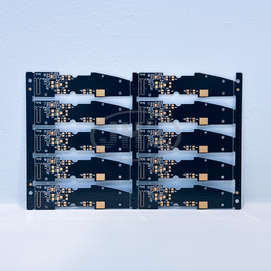
6 Layer 1-Order HDI Precision Buried Blind Via PCB
Layers:6-Layer Line Width/Spacing:0.075mm Material:FR-4 Surface Finish: ENIG Thickness:0.8mm Application:Communication
 189-2464-6170
 szjhpcb@VIP.126.com
7×24 Engineer One-on-One Technical Support
Juehui over 10 years of high-layer precision PCB technology, focusing on High Multilayer PCB R&D and manufacturing. High wiring density, strong signal integrity and low-loss characteristics, meeting mass production and prototyping needs for complex systems including medical devices, industrial control boards, automotive electronics and communication terminals.
Layers:6-Layer Line Width/Spacing:0.075mm Material:FR-4 Surface Finish: ENIG Thickness:0.8mm Application:Communication
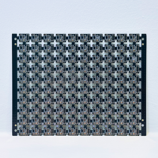
Layers:6-Layer Line Width/Spacing:0.075mm Material:FR-4 Surface Finish: ENIG Thickness:1.0mm Application:Micro Display

Layers:14-Layer Line Width/Spacing:0.2mm Material:FR-4 Surface Finish: ENIG Thickness:2.5mm Application:High-end Power Supplies

Layers:22-Layer Line Width/Spacing:0.076mm Material:FR-4 Surface Finish: Thickness:2.8mm Application:AI High‑Speed Server
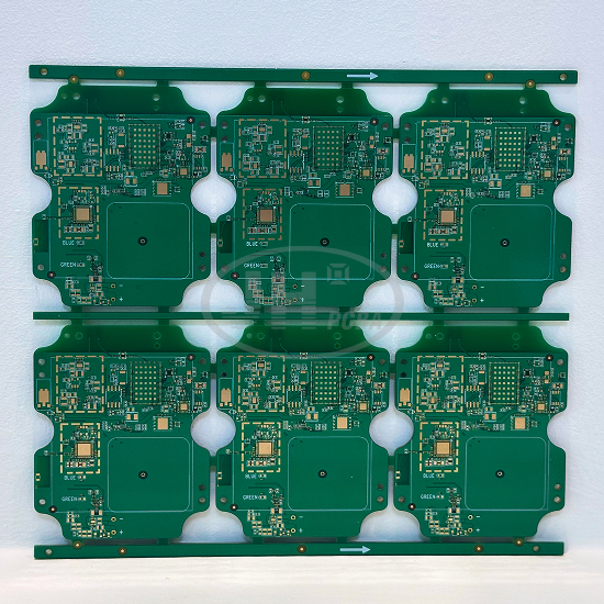
Layers:6层 Line Width/Spacing:0.075mm Material:FR-4 Surface Finish: ENIG Thickness:1.6mm Application:Communication Field

Layers:10-Layer Line Width/Spacing:0.1mm Material:FR-4 Surface Finish: ENIG 2U" Thickness:1.6mm Application:Automotive
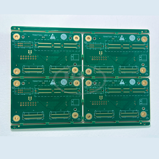
Layers:6-Layer Line Width/Spacing:0.1mm Material:Panasonic M6 Surface Finish: ENIG Thickness:2.4mm Application:Communication

Layers:6-Layer Line Width/Spacing:0.1mm Material:High Tg FR-4 Surface Finish: ENIG Thickness:1.6mm Application:Automotive
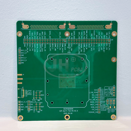
Layers:6-Layer Line Width/Spacing:0.1mm Material:4350B Surface Finish: ENIG Thickness:1.6mm Application:Industrial RF Circuit Board
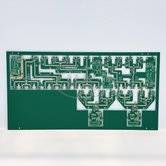
Layers:6-Layer Line Width/Spacing:0.2mm Material:Rogers4350B Surface Finish: ENIG Thickness:1.2mm Application:High Frequency RF Circuit Board

Layers:6-Layer Line Width/Spacing:0.1mm Material:FR-4 Surface Finish: ENIG Thickness:1.6mm Application:Medical Robot
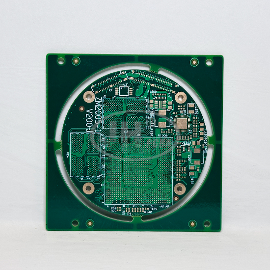
Layers:10-Layer Line Width/Spacing:0.07mm Material:FR-4 Surface Finish: ENIG Thickness:1.6mm Application:Aviation Navigation

Layers:4-Layer Line Width/Spacing:0.15mm Material:FR4+PP+PI Surface Finish: ENIG Thickness:1.6mm Application:AI Control System Integration

Layers: Line Width/Spacing:0.09mm Material:FR-4 Surface Finish: HASL‑Lead‑Free Thickness:1.6mm Application:Network Communication

Layers:12-Layer Line Width/Spacing:0.067mm Material:FR-4 Surface Finish: ENIG Thickness:2.0mm Application:High‑Speed Communication

Layers:12-Layer Line Width/Spacing:0.11mm Material:FR-4 Surface Finish: ENIG Thickness:1.6mm Application:High-Frequency Data PCB

Layers:10-Layer Line Width/Spacing:0.08mm Material:PP+PI Surface Finish: ENIG Thickness:0.12mm Application:Patient Monitor
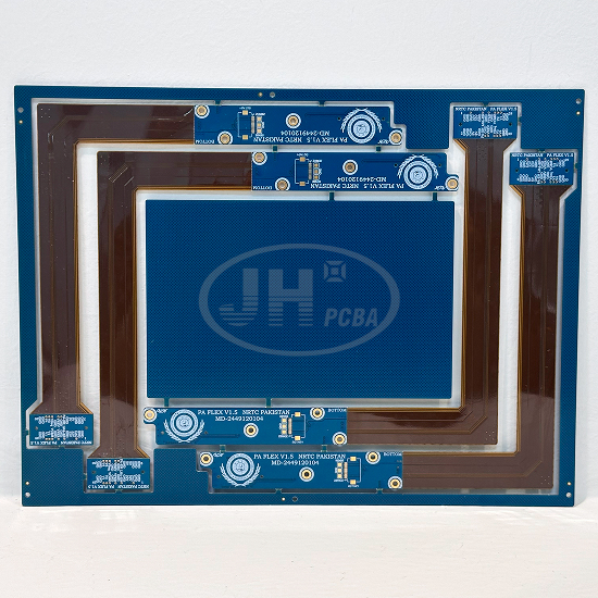
Layers:8-Layer Line Width/Spacing:0.1mm Material:PP+PI Surface Finish: Electroplated Hard Gold Thickness:0.15mm Application:Aerospace & Defense

Layers:8-Layer Line Width/Spacing:0.19mm Material:FR-4 Surface Finish: ENIG Thickness:3.2mm Application:BMS Balancing Main Controller
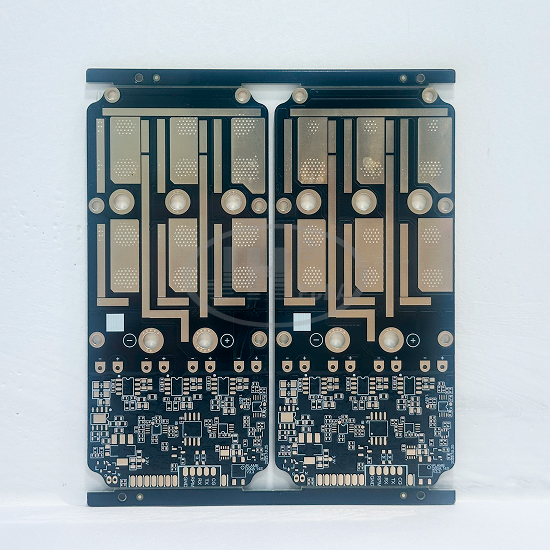
Layers:8-Layer Line Width/Spacing:0.29mm Material:FR-4 Surface Finish: ENIG Thickness:2.6mm Application:Energy Storage Power Supply

Layers:6-Layer Line Width/Spacing:0.152mm Material:Shengyi S1000-H Surface Finish: OSP+ENIG Thickness:1.6mm Application:Server & Storage
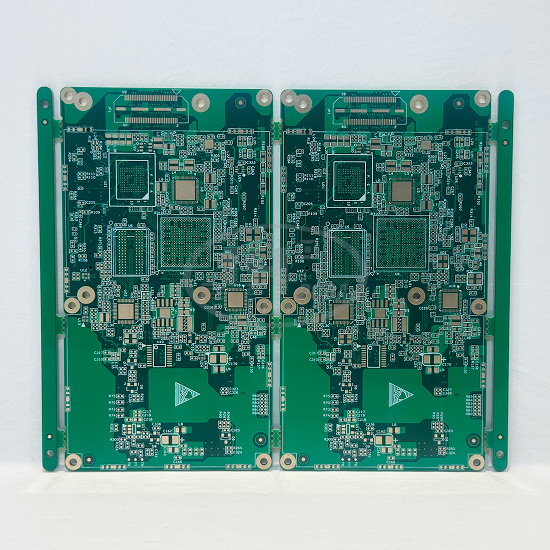
Layers:12-Layer Line Width/Spacing:0.11mm Material:FR-4 Surface Finish: Thickness:2.0mm Application:Industrial Control & Communication
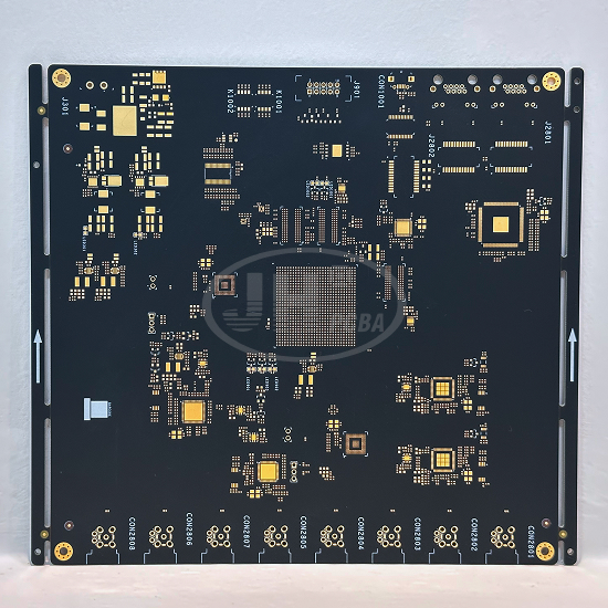
Layers:12-Layer Line Width/Spacing:0.08mm Material:FR-4 Surface Finish: ENIG Thickness:2.0mm Application:Automotive Electronics
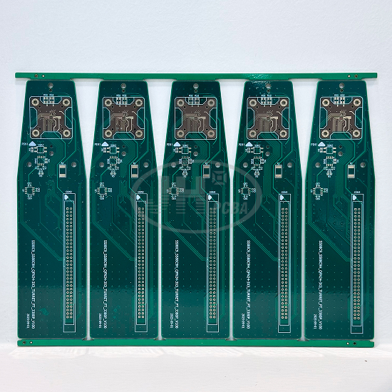
Layers:6-Layer Line Width/Spacing:0.15mm Material:FR-4 Surface Finish: ENIG Thickness:3.0mm Application:High-End Industrial Measurement & Control

Layers:8-Layer Line Width/Spacing:0.12mm Material:FR-4 Surface Finish: ENIG Thickness:1.6mm Application:Premium Intelligent Control
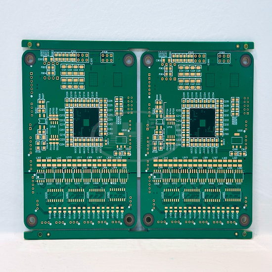
Layers:6-Layer Line Width/Spacing:0.095mm Material:FR-4 Surface Finish: ENIG Thickness:2.4mm Application:Industrial Robot
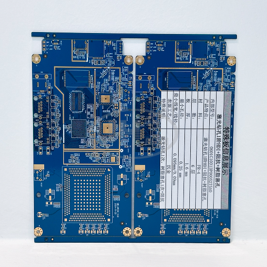
Layers:6-Layer Line Width/Spacing:0.095mm Material:FR-4 Surface Finish: ENIG Thickness:1.6mm Application:Industrial Ethernet
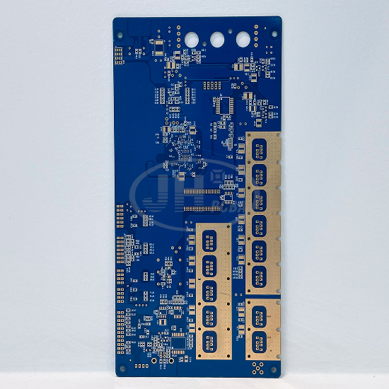
Layers:10-Layer Line Width/Spacing:0.15mm Material:FR-4 Surface Finish: ENIG Thickness:1.6mm Application:Industrial Servo Drive
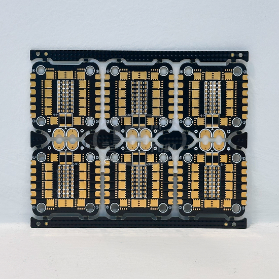
Layers:6-Layer Line Width/Spacing:0.203mm Material:FR-4 Surface Finish: ENIG Thickness:1.6mm Application:Energy Storage System
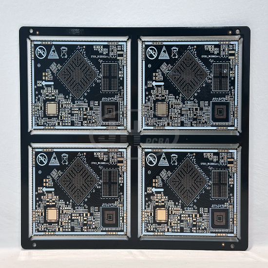
Layers:8-Layer Line Width/Spacing:0.1mm Material:FR-4 Surface Finish: ENIG Thickness:1.2mm Application:Edge Computing
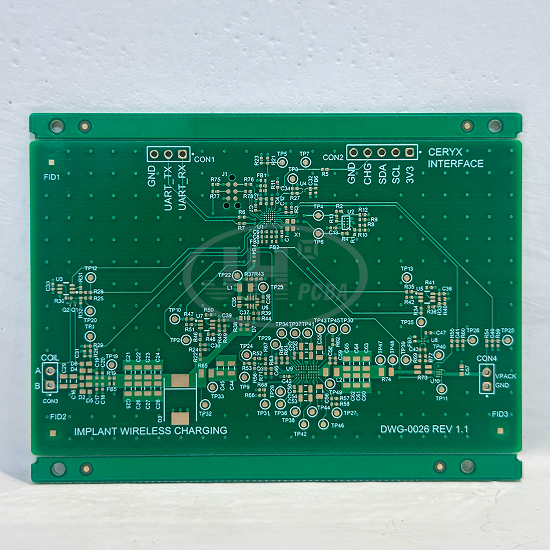
Layers:4-Layer Line Width/Spacing:0.23mm Material:FR-4 Surface Finish: ENIG Thickness:1.6mm Application:Implantable Medical Devices
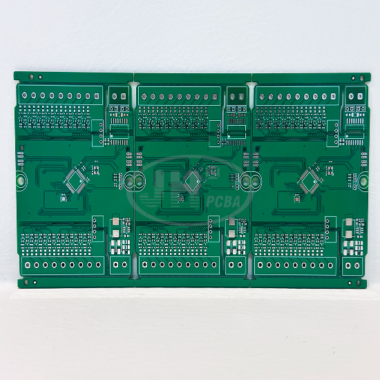
Layers:4-Layer Line Width/Spacing:0.2mm Material:FR-4 Surface Finish: HASL Thickness:1.6mm Application:Industrial Multi-IO Control Board
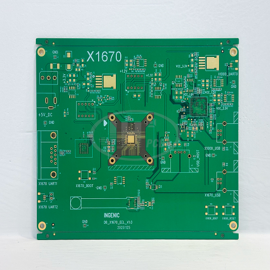
Layers:6-Layer Line Width/Spacing:0.13mm Material:FR-4 Surface Finish: ENIG Thickness:2.0mm Application:Industrial AI Vision
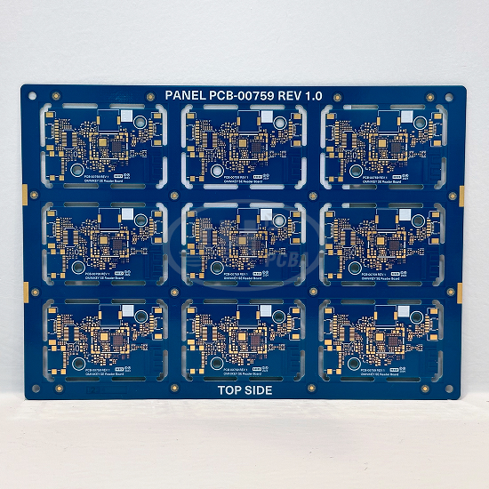
Layers:8-Layer Line Width/Spacing:0.145mm Material:FR-4 Surface Finish: ENIG Thickness:1.0mm Application:Smart Card Reading Access Control
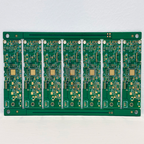
Layers:6-Layer Line Width/Spacing:0.01mm Material:FR-4 Surface Finish: ENIG 2U" Thickness:1.0mm Application:Portable Medical Devices

Layers:6-Layer Line Width/Spacing:0.18mm Material:FR-4 Surface Finish: ENIG Thickness:1.6mm Application:Power Mainboard
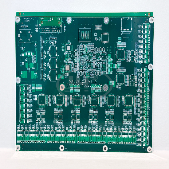
Layers:12-Layer Line Width/Spacing:0.15mm Material:FR-4 Surface Finish: HASL Thickness:3.0mm Application:Multi-channel Solenoid Valve Board
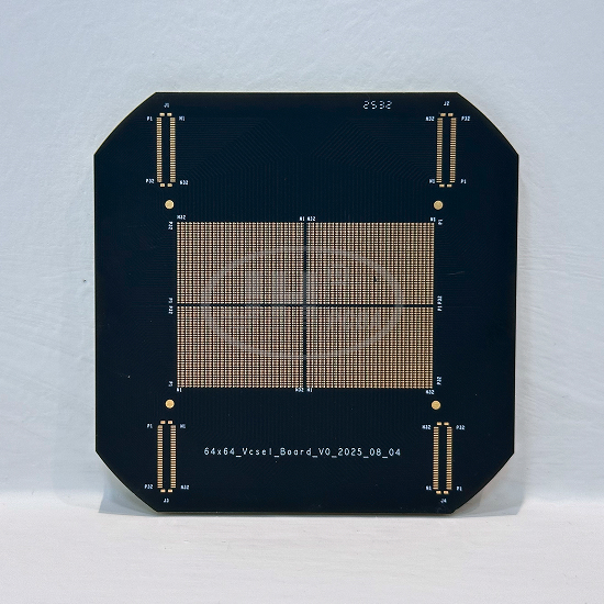
Layers:4-Layer Line Width/Spacing:0.22mm Material:FR-4 Surface Finish: ENEPIG Thickness:5.0mm Application:Optoelectronics Industry
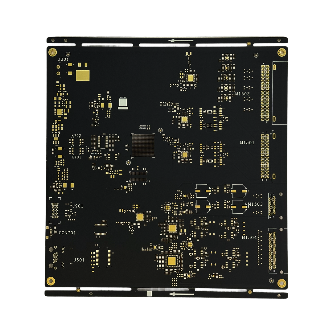
Layers:12-Layer Line Width/Spacing:0.08mm Material:TU872 Surface Finish: ENIG Thickness:2.0mm Application:Automotive Electronics

Layers:14-Layer Line Width/Spacing:0.11mm Material:TU872 Surface Finish: ENIG,2U” Thickness:2.0mm Application:Automotive Electronics

Providing Truly Reliable PCB & PCBA Products
 Grade-A Materials
 ISO Certified
 One-on-One Service
 Fast 8-Hour Delivery

Please fill in "Phone" before submitting
24H Hotline 189-2464-6170 is always here for you! PCB Quote


Submitted Successfully
Our engineer will contact you at within 2 hours. Please keep your phone available!
