 189-2464-6170
 szjhpcb@VIP.126.com

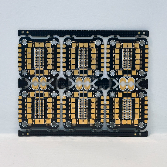
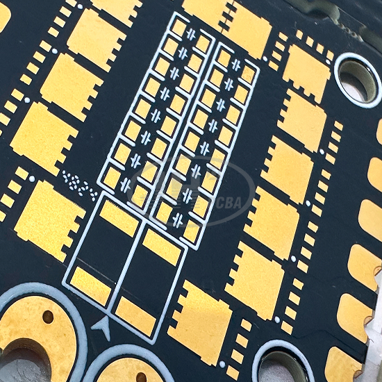
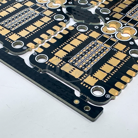
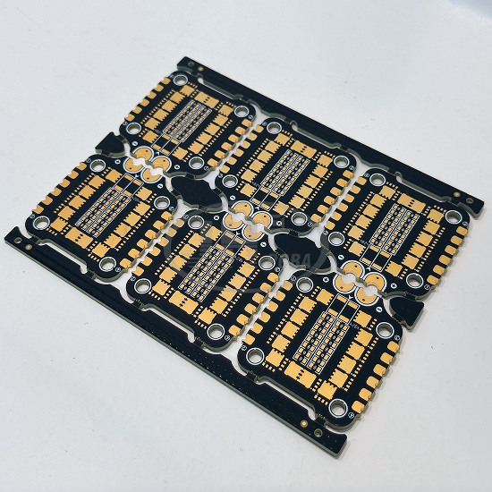
 Material: FR-4
Product Detail
1-Stage Mechanical HDI Structure for Higher Routing Density
Blind and buried via interconnections free up routing space. Power loops, detection sampling and protection circuits can be integrated within a compact area, supporting miniaturized design of compact power modules.
Dual Resin Plugging for Enhanced Reliability
Separate filling and planarization processes are applied to different buried vias, thoroughly eliminating solder entrapment, voids and moisture ingress during SMT soldering. Multi-layer power and ground layers offer stable high-current carrying capacity with lower voltage drop and less heat generation.
Advantages of Edge Castellated Hole Structure
Castellated holes enable direct soldering and edge-mounted assembly without connectors, simplifying the overall mechanical structure. Strict process control prevents burrs, copper lifting and exposed copper corrosion, delivering consistent and reliable solder joints.
ENIG Process Optimized for High-Current Precision Soldering
Large-area power pads and BGA pads remain flat, anti-oxidation and anti-tarnish. The surface resists discoloration after multiple reflow cycles. It provides better stability for high-current soldering and component rework compared with HASL, ideal for power devices operating continuously over long periods.
Linked Panel Design for Mass Production
Multi-up panel layout is compatible with high-speed inline SMT manufacturing. Low stress during depaneling avoids chipping on castellated holes, significantly improving mass production yield and reducing unit cost.
6-Layer Multi-Layer Shielding for Superior Anti-Interference Performance
Well-structured multi-layer power and ground planes deliver strong EMI suppression and excellent noise immunity for sampling signals, ensuring accurate and stable battery overvoltage and overcurrent protection.



