189-2464-6170
 szjhpcb@VIP.126.com

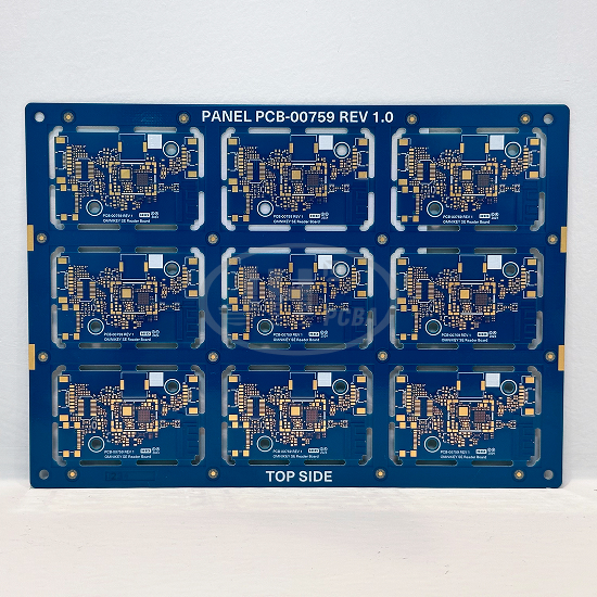
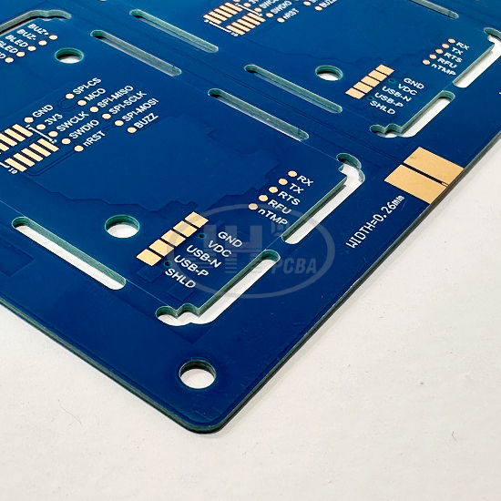
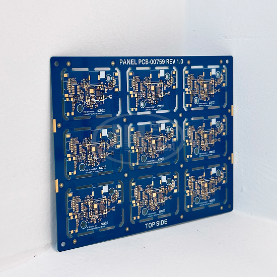
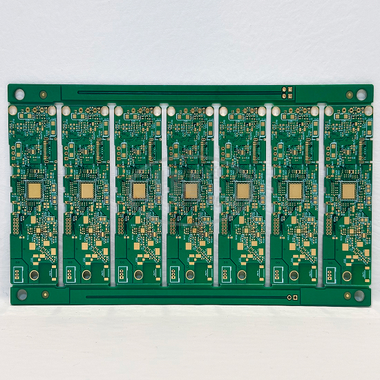
 Material: FR-4
Product Detail
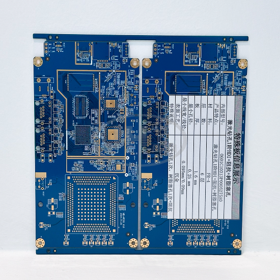
3-Stage Triple Laser Blind Via Structure
It realizes progressive blind via interconnection from shallow layers to middle layers and inner layers, greatly improving wiring density. Compatible with large-pin-count BGA packages, it saves board space and meets the design requirements of miniaturized high-end modules.
Buried Via Resin Plugging Process
Buried vias are fully filled and planarized. No solder trapping or bubbling occurs during SMT soldering to boost assembly yield. The board gains improved moisture and corrosion resistance for enhanced long-term reliability of multi-layer structures.
Full-Process Precise Controlled Impedance
Closed-loop control of trace width, copper thickness and dielectric thickness throughout production. Excellent impedance consistency for high-speed differential and single-ended signals delivers superior signal integrity, reducing interference and signal attenuation.
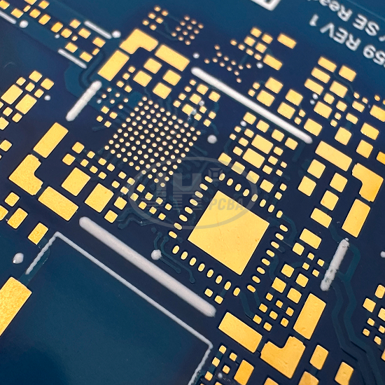
ENIG Surface Finish
Flat BGA pads feature anti-oxidation and anti-tarnish performance. Pads will not darken after multiple reflow cycles, offering far higher reliability for ball mounting and precision chip soldering compared with HASL.
8-Layer Multi-Step Lamination
Internal stress is fully released to minimize warpage and deformation of thin boards, satisfying flatness requirements for high-precision SMT assembly equipment.
Advantages of Miniaturization & High Density
HDI micro-vias enable finer traces and smaller pad sizes. More circuit functions can be integrated within limited dimensions, matching the miniaturization trend of high-end intelligent identification and communication products.