189-2464-6170
 szjhpcb@VIP.126.com

 Material: FR-4
Product Detail
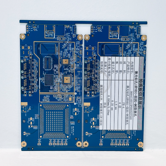
6 Layer 1-Stack HDI PCB with Buried & Blind Via | High Precision BGA Resin Plugged Circuit Board for Micro Display
Product Overview
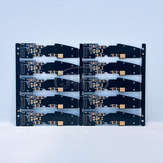
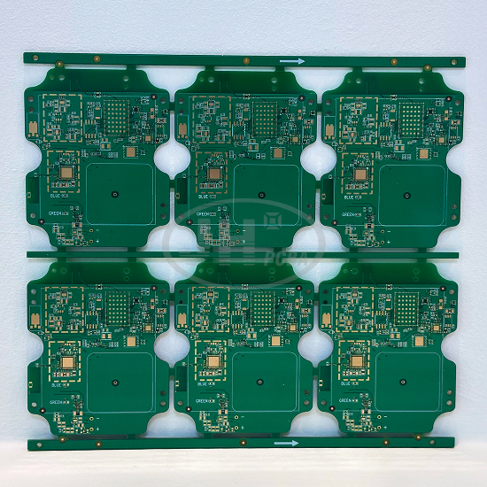
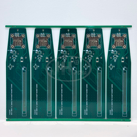
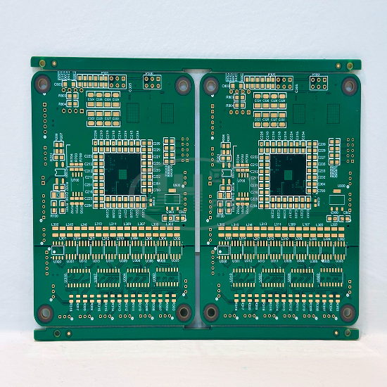
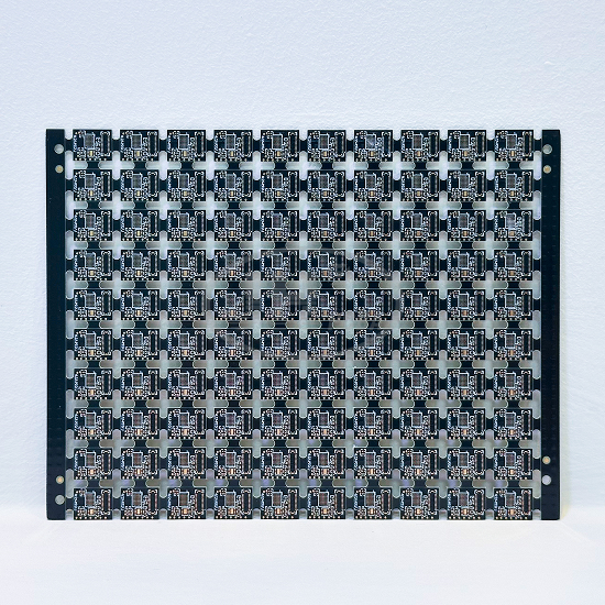
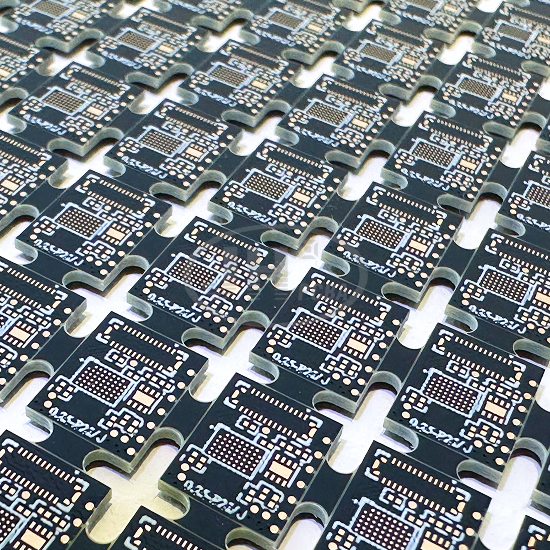
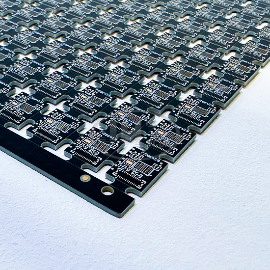
This is a 6-layer 1st order HDI high-density interconnect PCB with buried and blind vias. It is made of high Tg FR4 substrate with board thickness of 1.0mm. Adopting UV laser microvia technology, the minimum hole size reaches 0.075mm, minimum trace/space 3mil/3mil. Finished with ENIG surface treatment, it supports BGA pad-on-via and resin plug hole design. Manufactured in panel array with tab-routing (stamp hole), this PCB is specially developed for micro display modules.
HDI buried & blind via structure greatly shortens signal path and reduces signal interference. Ultra-fine trace layout realizes dense wiring for BGA chips within limited space. Resin plug technology ensures flat surface, improves SMT assembly and BGA soldering yield. Widely used in AR/VR micro-display, micro-projector, wearable micro-display and other precision optoelectronic products.
Specifications
- Layers: 6 layers, 1st order HDI (combination of buried vias & laser blind vias)
- Material: High Tg FR4 epoxy glass laminate
- Board Thickness: 1.0mm
- Minimum Hole Size: 0.075mm (UV laser drilling)
- Min Trace / Space: 3mil / 3mil
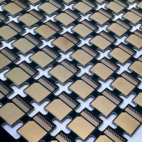
- Surface Finish: ENIG (Electroless Nickel Immersion Gold)
- Special Process: BGA pad on via, resin plugged holes, tab-routing panel
- Flame Retardant: UL94 V-0
Process Features
1. 1st order HDI buried & blind via: Laser blind vias connect outer layer and sub-layer, buried vias realize inner-layer interconnection, saving routing space for miniaturization and high density design.
2. 0.075mm laser microvia & 3mil ultra-fine trace: Equipped with high-end UV laser drill and high-precision exposure & etching line, stable mass production for microvia & fine line for dense BGA pins.
3. Resin plug & planarization: Vias fully filled with resin and ground flat, prevent solder ball and cavity issue, guarantee BGA pad coplanarity.
4. ENIG Gold Plating: Flat pad surface, good oxidation resistance, suitable for rework soldering of precision BGA chips.
5. Tab-routing panel design: Panel production for automatic SMT assembly, easy depaneling, improve customer’s SMT productivity.
Application Fields
✅ Micro display, AR/VR micro display module
✅ Micro OLED / LCD driver control board
✅ Micro projector, optical sensor main board
✅ Wearable device micro display PCB
✅ Compact precision optoelectronic module circuit board
Advantages of Juehui Weiye Circuit
Juehui Weiye Circuit focuses on R&D and manufacturing of high-end precision PCB. We have full mass production capability for HDI high-density boards, including DFM pre-analysis, laser drilling, resin plugging and final inspection.
1. Equipment: UV laser drill, auto exposure machine, continuous electroplating line, AOI optical inspection, flying probe tester to guarantee yield of fine lines & micro vias.
2. Quality Control: Every PCB undergoes AOI scan and flying probe electrical test for open/short and line width defect. Thermal shock, impedance and warp inspection strictly control HDI board warpage.
3. Flexible Delivery: Fast prototype, small & medium batch and mass panel orders available. Our engineers provide free DFM review to optimize BGA and blind via design, reduce R&D risk.
Certifications
✅ ISO9001 Quality Management System
✅ ISO13485 Medical Device Quality Management System
✅ RoHS Compliance
✅ REACH Registration
✅ UL Safety Certification
Order Information
Please send Gerber files, stack-up requirement, impedance specification and surface finish requirement for quotation and manufa
📞 Tel:+86 189-2464-6170
📧 Email:szjhpcb@vip.126.com
🌐 Official Website:https://www.szjhpcba.com/