189-2464-6170
 szjhpcb@VIP.126.com


 Material: FR-4
Product Detail
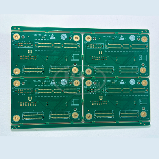
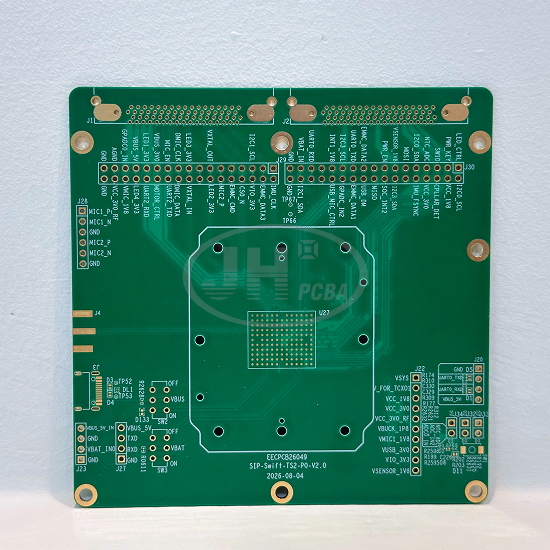
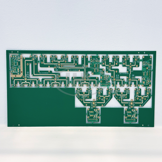
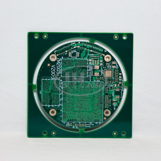
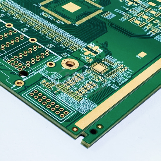
6 Layer HDI Resin Plug Hole PCB | ENIG Edge Gold Plated Communication Mainboard
Introduction
Looking for reliable high-speed PCB for your network switch and industrial communication project? This 6-layer resin plugged hole PCB from Juehui Weiye Circuit is an ideal solution.
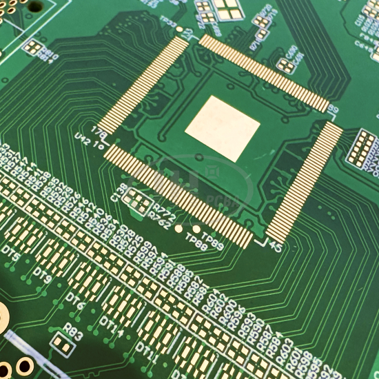
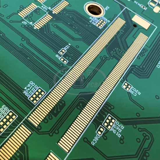
Built on high TG FR4 material with 1.6mm thickness, 180×239mm outline, the board features ENIG on pads plus edge gold plating for shielding ground. It is engineered with dense BGA fanout and SFP high-speed interface routing. Resin plugging removes via stubs, while controlled impedance differential traces keep signal clean at high data rate.
Key Parameters
Layer count: 6
Board thickness:1.6mm
Dimension:180*239mm
Base material: High Tg FR4 Tg170,
UL94 V0 flame retardant
Surface treatment: Electroless Nickel Immersion Gold + selective edge gold plating
Minimum drill:0.2mm
Min line/space:0.10mm /0.10mm
Featured craft: Resin filled & planarized vias, impedance control, differential length matching, BGA fine line routing
Solder mask: Green, white silk screen
Certificate: RoHS
Why Choose This Design
✅ Resin plug via technology: No stub, less signal loss, perfect flat surface for BGA assembly
✅ Strict impedance control: TDR test for every batch, stable differential signal performance
✅ Edge gold shielding design: Improve EMC performance for industrial communication device
✅ Large size multi-layer process: Advanced shrinkage control, low layer shift for dense circuits
✅ High quality ENIG finish: Anti-oxidation, multiple rework cycles, stable soldering performance
Typical Application
Industrial ethernet switch, 5G communication gateway, optical module controller, high speed data capture board, industrial control main unit.
About Juehui Weiye Circuit
We are a professional PCB manufacturer located in Shenzhen, China. We focus on complex PCB including resin plug PCB, high speed impedance PCB, HDI, multi-layer & heavy copper PCB.
We accept prototype and bulk order, support Gerber, ODB++ design files. Our engineering team provides free DFM check and stack-up optimization. All boards are inspected by AOI and electrical test before shipment.
Contact us today to get your quotation and sample lead time!
Ordering Instructions
Please provide Gerber files, stack-up requirements, impedance specifications and surface finish requirements for quotation and manufacturability evaluation. Board material, layer count, board thickness and surface treatment can be customized as required.
📞 Tel: +86 189-2464-6170
📧 Email: szjhpcb@vip.126.com
🌐 Website: https://www.szjhpcba.com