189-2464-6170
 szjhpcb@VIP.126.com

 Material: FR-4
Product Detail
2-Stage Dual Laser Blind Vias for Ultra-High Routing Density
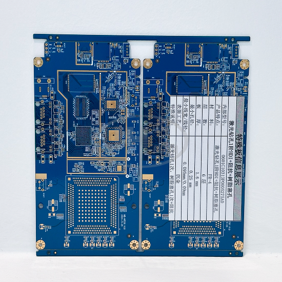
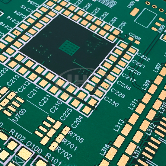
Two tiers of stepped laser blind vias greatly improve interlayer connection efficiency. The outer layer can accommodate numerous fine-pin BGAs and multi-channel IO interfaces, enabling complex multi-channel circuit layout within limited board space to meet high-density expansion requirements of industrial control equipment.
Resin-Filled Buried Vias Enhance Long-Term Stability
Planarized buried vias completely avoid solder entrapment and moisture-induced delamination during soldering. Continuous multi-layer power and ground planes boost high-current carrying capacity with low voltage drop and minimal heat generation during prolonged continuous operation.
Precision Process for Ultra-Fine Traces
Minimum trace width reaches 0.095 mm, supporting dense pin header routing and peripheral circuits around ICs. Shorter signal traces reduce transmission interference, ideal for multi-channel parallel signal acquisition applications.
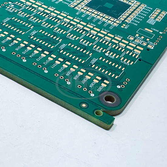
High-Rigidity Structure with 2.4mm Thick Board
The substrate features strong bending and deformation resistance, delivering excellent shock resistance after integration. It maintains stable geometry in harsh industrial environments. Reinforced mounting holes suit frequent assembly operations.
ENIG Process Optimized for Dense Soldering
Peripheral pin header pads and central BGA pads resist oxidation and tarnishing. It achieves high yield for ball mounting and through-hole soldering after multiple reflow cycles with reliable rework performance.
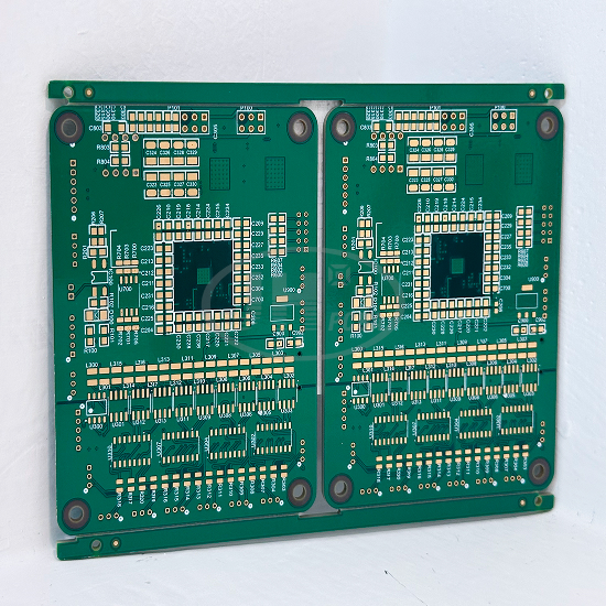
Dual-Up Panel Design for Mass Production
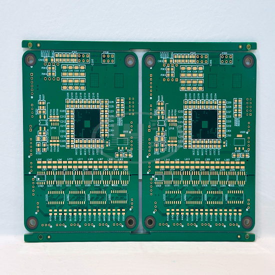
Two boards arranged in one panel for each production run, compatible with high-speed SMT production lines. Low stress occurs during depaneling, raising manufacturing efficiency and reducing unit production cost.