189-2464-6170
 szjhpcb@VIP.126.com



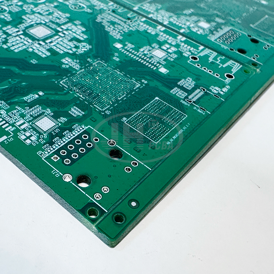
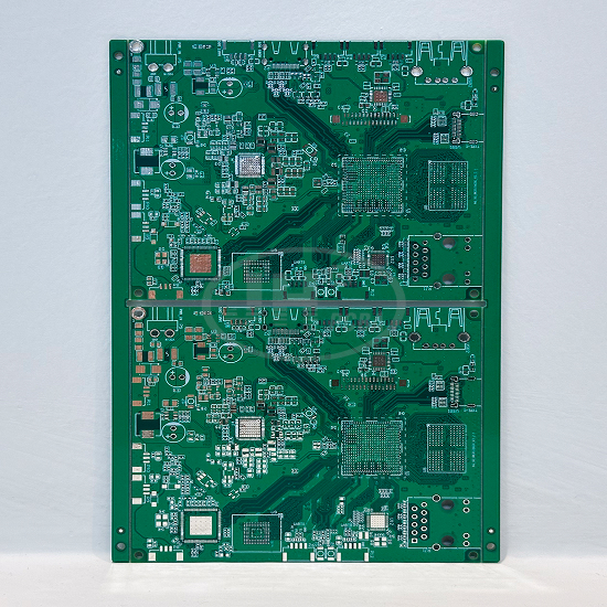
 Material: FR-4
Product Detail
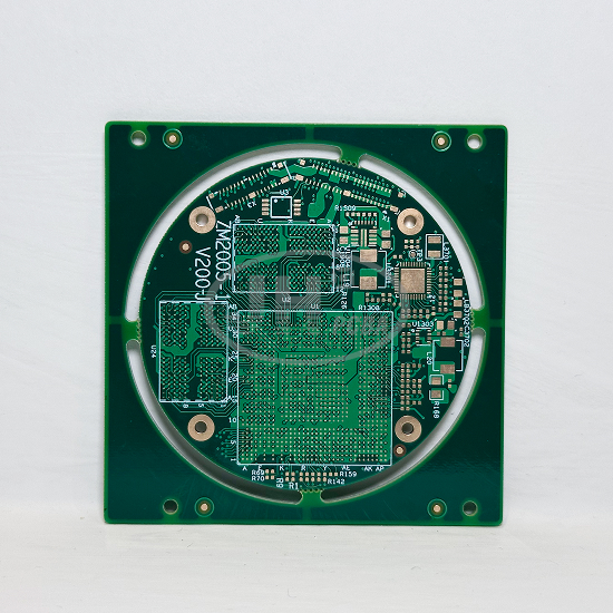
8‑Layer Layer‑Stack Architecture
Isolated power and ground layers provide shielding to suppress EMI electromagnetic interference and ensure excellent high‑speed signal integrity, supporting dense routing for large BGA chips.
Lead‑Free HASL Surface Finish
RoHS‑compliant lead‑free finish with good solder wettability and moderate cost. Highly compatible with high‑volume SMT assembly and convenient for rework.
1.6 mm Standard Board Thickness
Sufficient mechanical rigidity and warpage resistance, offering great versatility for system mechanical assembly.
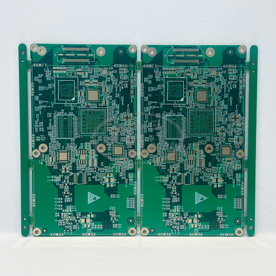
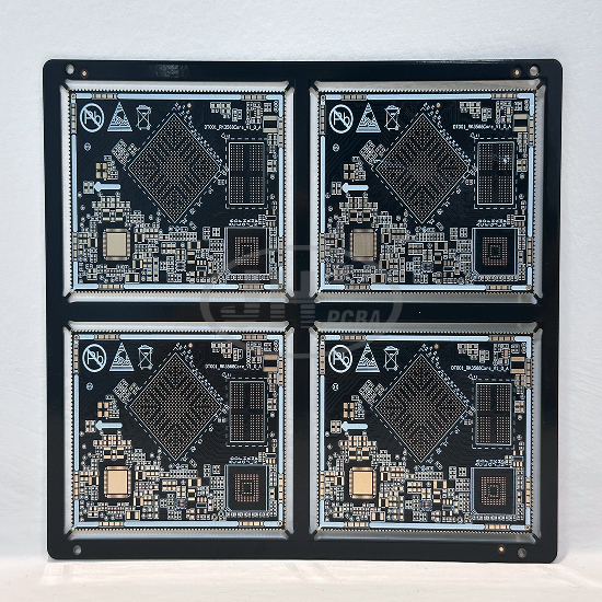
V‑Cut Two‑Up Panel Design
Optimized for fully‑automated high‑volume SMT production. Easy depaneling improves manufacturing efficiency and reduces assembly cost.
Customizable Controlled Impedance
Impedance tuning available for USB, Ethernet port, DDR and high‑speed differential signal traces.
High‑Reliability Lamination Process
Robust inter‑layer bonding prevents delamination and blistering. Excellent thermal‑shock resistance and stable long‑term performance.
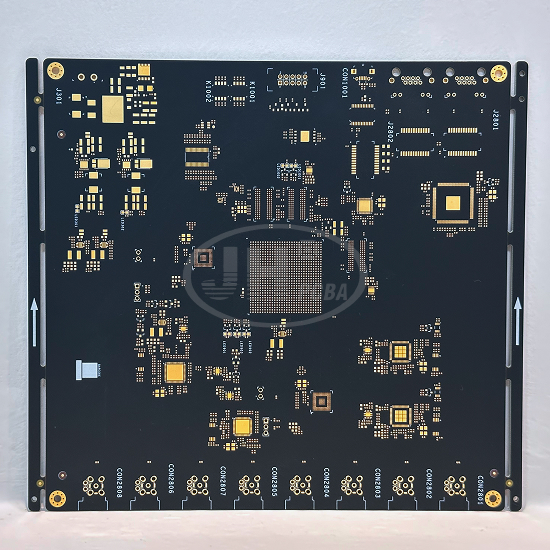
High‑Density Routing Capability
Supports fine‑pitch BGA and dense via layout to reduce overall PCB footprint of end devices.