189-2464-6170
 szjhpcb@VIP.126.com

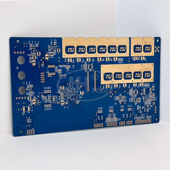
 Material: FR-4
Product Detail
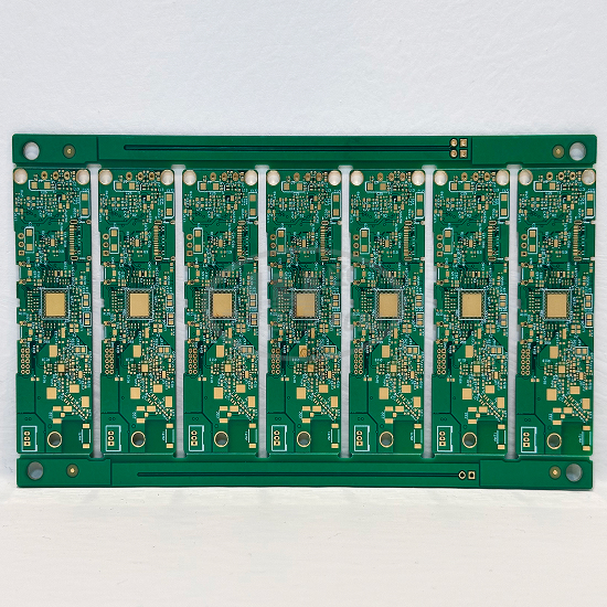
10-Layer 1-Stage HDI Structure for Greatly Improved Routing Density
Laser blind vias connect the outer layer to the adjacent inner layer, freeing up more inner-layer routing space. It supports compact multi-pin BGAs and reduces board dimensions, ideal for compact high-power industrial control products.
Higher Reliability with Resin-Filled Buried Vias
Buried vias are filled and planarized to avoid solder entrapment and bubbling during SMT assembly, while delivering moisture and corrosion resistance. The multi-layer power and ground planes for high-current applications feature low voltage drop and low heat generation, suitable for multi-channel power circuits.
Closed-Loop Controlled Impedance Throughout Production
Full-process control over trace width, copper thickness and dielectric thickness ensures excellent high-speed differential signal integrity with reduced crosstalk and attenuation, and outstanding noise immunity for analog signals.
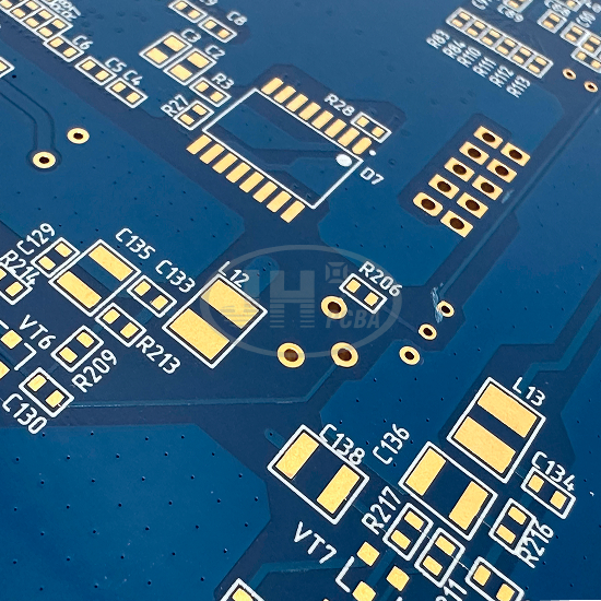
ENIG Process Optimized for Precision Soldering
Flat BGA and small pads feature oxidation and tarnish resistance. The surface avoids discoloration after multiple reflow cycles and offers superior stability for fine-pitch IC soldering and rework compared with HASL.
Low Deformation via Stepwise Lamination for 10 Layers
Board internal stress is fully relieved to achieve high flatness, meeting high-precision mass assembly requirements of high-speed SMT equipment and delivering high production yield.
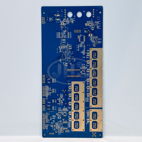
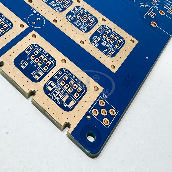
Power-Oriented Design with Large Copper Areas
Continuous multi-layer power and ground planes provide excellent heat dissipation and high current carrying capacity, along with effective EMI shielding, suited for multi-channel power driver applications.