189-2464-6170
 szjhpcb@VIP.126.com

 Material: FR-4
Product Detail
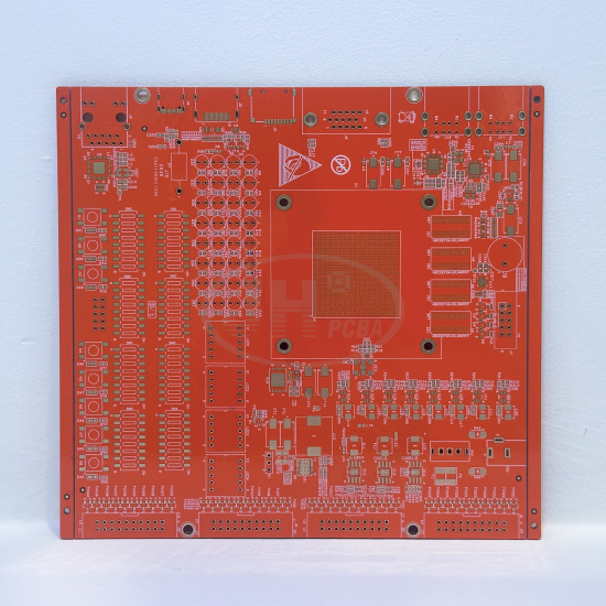
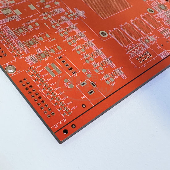
10-Layer HDI PCB with Buried & Blind Vias | Orange Solder Mask High-Density BGA Chip Test Mainboard
Product Overview
This 10-layer HDI PCB with buried and blind vias is developed for semiconductor chip testing and high-speed FPGA verification equipment. Adopting High Tg FR4 substrate, finished board thickness 2.0mm, dimension 160×170mm, with 1st-order HDI stack-up of buried & blind vias. Equipped with custom orange solder mask ink, resin plugging process and ENIG surface finish.
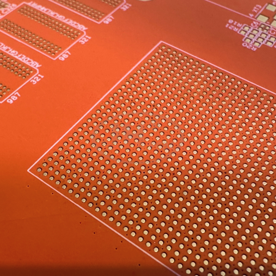
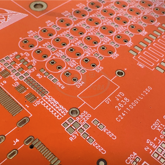
A large-area BGA array pad is designed at the center of the board. 0.1mm laser blind vias together with 0.075mm ultra-fine traces realize high-density fanout for massive I/O signals. The orange solder mask facilitates visual inspection and maintenance of test fixtures. The 2.0mm thick board ensures rigidity for large-size panel and anti-deformation performance, suitable for SMT assembly with dense components on both sides. Widely applied in semiconductor ATE automatic test equipment, high-speed FPGA development boards and industrial multi-channel signal acquisition instruments.
Core Specifications
Layers : 10 Layers, 1st-order HDI PCB with Buried & Blind Vias
Substrate : High Tg FR-4 fiberglass epoxy laminate
Finished Board Thickness : 2.0 mm
Dimension : 160*170 mm
Minimum Aperture : 0.1 mm (Laser Blind Via)
Min. Line Width / Line Space :0.075 mm / 0.075 mm (3mil / 3mil)
Surface Finish : ENIG (Electroless Nickel Immersion Gold)
Solder Mask Ink : Custom Orange Special Solder Mask Ink
Featured Processes : 1st-order HDI buried & blind vias, resin plugging, high-density BGA fanout
Flammability Rating : UL94-V0
Application Fields : Semiconductor chip test equipment, industrial automation, high-speed signal acquisition, FPGA embedded main control
Applicable Products : ATE semiconductor automatic test mainboard, high-speed FPGA verification board, multi-channel industrial signal acquisition board, main control board for automatic testing instruments
Material Description
High Tg FR4 fiberglass epoxy laminate is selected as substrate. It features excellent heat resistance and minimal deformation under multiple reflow cycles. The 2.0mm board thickness guarantees structural rigidity for the 160×170mm large panel and reduces warpage risk during SMT assembly. High-adhesion PP prepreg is used between layers to prevent delamination after multiple lamination cycles.
Custom orange solder mask ink is adopted with strong adhesion, acid & alkali resistance, high temperature resistance and stable color difference. Compared with conventional green solder mask, the orange surface allows engineers to visually inspect traces and test points more conveniently, simplifying fault inspection for chip test fixtures. Meanwhile, it protects precision copper traces against oxidation and short circuit.
PCB Manufacturing Advantages
1. 1st-order HDI Buried & Blind Via Technology: 0.1mm micro blind vias fabricated by laser drilling to interconnect top and inner layers. Buried vias are made by mechanical micro-hole drilling plus resin plugging, filled, ground and planarized to eliminate soldering voids. It enables high-density fanout of BGA pins and greatly improves routing density.
2. Ultra-fine Precision Traces: Stable production of 0.075mm/0.075mm fine line width & space to meet high-speed signal transmission and massive I/O routing requirements. Impedance is strictly controlled to ensure signal integrity.
3. Custom Orange Solder Mask Process: Printing with special orange ink, color difference and ink thickness are well controlled, balancing trace protection and visual maintenance.
4. ENIG BGA Pads: Flat and uniform pads with high flatness over BGA array area, good oxidation resistance and solderability. Compatible with precision BGA & QFN device soldering, delivering stable contact resistance under repeated probe testing.
5. Large Panel Anti-Warpage Control: Optimized multi-layer multi-lamination process to solve the industry challenge of warpage on large-size 160×170mm HDI boards, improving SMT assembly yield.
6. Multi-stage Quality Inspection: 100% Flying Probe electrical continuity & insulation resistance test, AOI optical scanning, special visual inspection for BGA zones. Reliability tests such as thermal shock, damp heat and peel strength are available upon request.
PCB Application Scenarios
Main control board for semiconductor ATE automatic test equipment, high-speed FPGA development & verification board, motherboard for chip test fixtures, industrial multi-channel high-speed signal acquisition board, control board for high-end instruments & meters, core PCB for automated visual inspection equipment.
JUEHUI WEIYE CIRCUIT | Manufacturing Strength
Juehui Weiye Circuit is a professional original PCB manufacturer in China with full capability from prototype to mass production for high-layer HDI multi-layer PCBs. We focus on PCB solutions for semiconductor testing and high-speed instruments.
Our factory is proficient in 1st / 2nd order HDI buried & blind vias, resin plugging, custom color special solder mask and ultra-fine trace fabrication, specializing in large-size high-density BGA mainboard production.
We hold ISO9001 and ISO13485 medical device quality management system certifications. One-stop service is available from rapid prototyping to volume delivery.
All products comply with IPC-A-600 international standards. Material certificates and reliability test reports can be provided per batch, supporting customers for relevant certification of semiconductor equipment.
Ordering Instructions
Please provide Gerber files, stack-up requirements, impedance specifications and surface finish requirements for quotation and manufacturability evaluation. Board material, layer count, board thickness and surface treatment can be customized as required.
📞 Tel: +86 189-2464-6170
📧 Email: szjhpcb@vip.126.com
🌐 Website: https://www.szjhpcba.com