 189-2464-6170
 szjhpcb@VIP.126.com


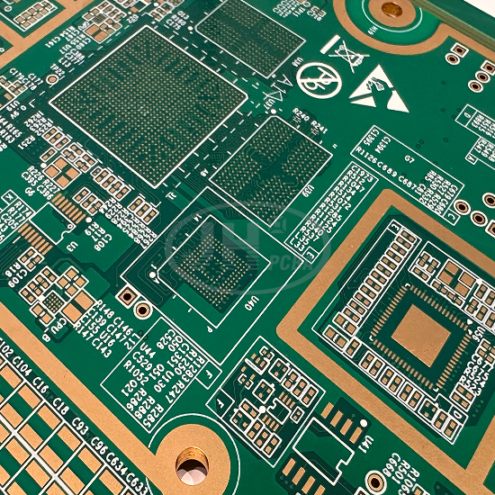
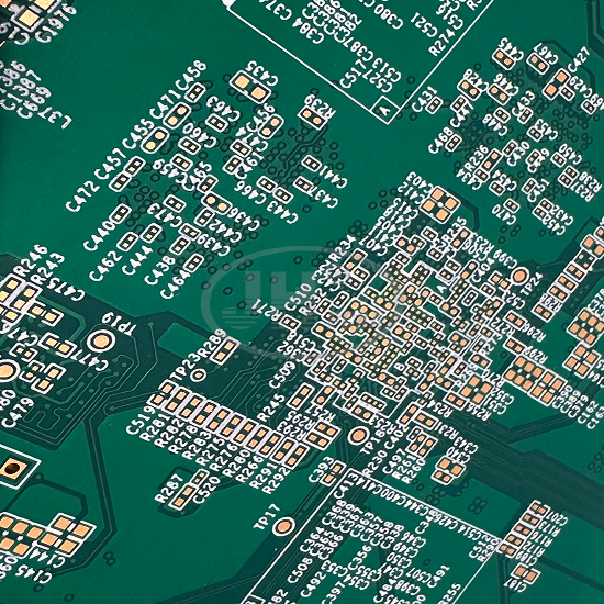
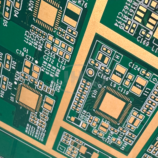
 Material: FR-4
Product Detail
Remove Excess Inner‑Layer Hole Stubs
Eliminates hole stubs to suppress reflection, crosstalk and resonance of high‑speed differential signals. It greatly improves signal quality for PCIe, DDR and high‑speed serial buses, meeting stringent timing requirements for high‑frequency and high‑speed applications.
Improved Multilayer Reliability via One‑Step Resin Plugging
Buried vias are fully filled and planarized to prevent solder trapping and bulging during SMT soldering. It delivers superior moisture and corrosion resistance and enhances thermal‑cycle stability for multi‑layer power / ground planes, avoiding open‑circuit risks caused by voids.
Full‑Process Precision Impedance Control
Closed‑loop process control over trace width, copper weight and dielectric thickness ensures high consistency for differential and single‑ended impedance. It reduces signal attenuation and interference, suitable for mixed‑signal designs combining high‑frequency RF and high‑speed digital circuits.
Immersion Gold for Large‑Size BGA Soldering
Flat, anti‑oxidation and anti‑sulfidation BGA array pads resist discoloration after multiple reflow cycles. It provides far higher reliability for ball‑mounting, fine‑pitch large‑chip soldering and rework compared with HASL.
12‑Layer Multi‑Step Lamination for Low‑Warpage Performance
Specially optimized to release internal stress of high‑layer‑count boards. It mitigates common defects including warpage, delamination and blistering. Excellent flatness supports high‑precision mass assembly by premium high‑speed SMT equipment.
Robust 2.0mm Thick‑Board Construction
High mechanical strength with excellent resistance against bending and deformation, ensuring stable long‑term operation for server...




