189-2464-6170
 szjhpcb@VIP.126.com

 Material: FR-4
Product Detail
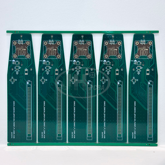
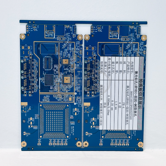
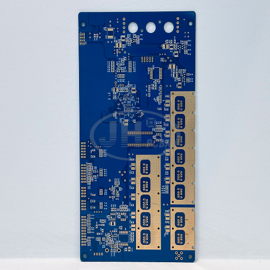
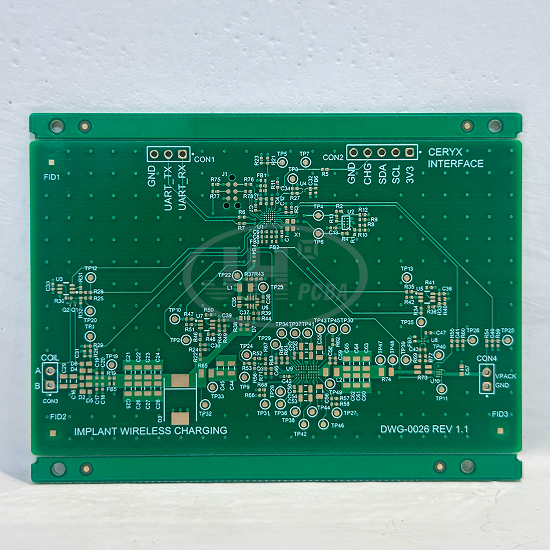
6-Layer 1-Order HDI High Density PCB | Precision Circuit Board for IoT Wireless Locator
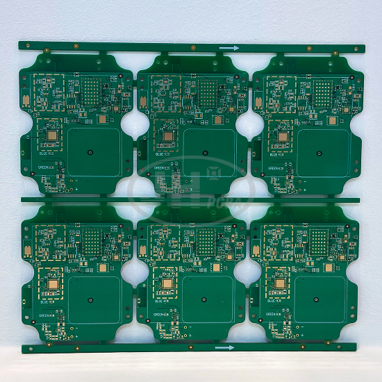
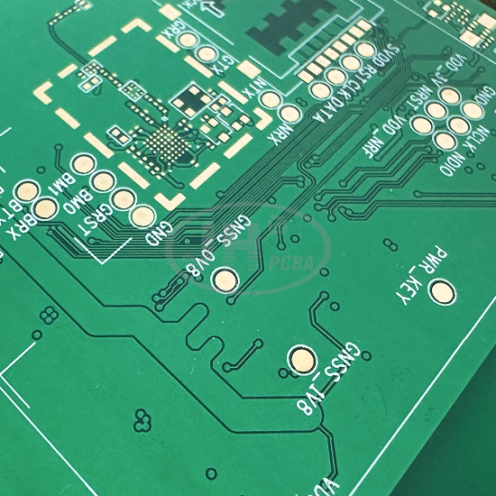
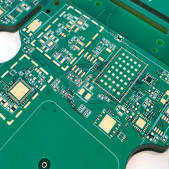
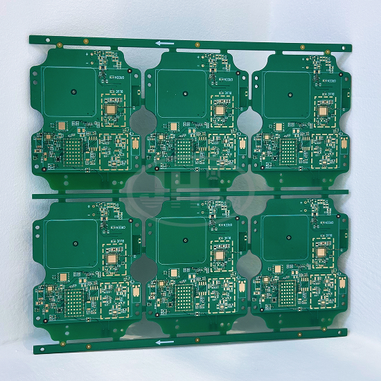
This 6-layer 1-order HDI high-density PCB, panel size 186×183mm, finished thickness 1.6mm. Adopted high TG FR4 substrate, green solder mask with ENIG surface finish, 6-up panel design. Custom developed for IoT GNSS wireless positioning terminal.With 1-order HDI laser microvia technology, laser blind vias directly connect BGA pads to achieve high routing density. The PCB integrates large antenna keep-out area, mixed RF & digital circuit. Isolated ground plane and controlled impedance reduce wireless signal interference. CNC custom contour with panel tooling holes, fully compatible with automatic SMT assembly line. Juehui Weiye customizes HDI multilayer PCB according to customer Gerber files, supporting impedance design, blind & buried via process, one-stop service from rapid prototype to mass production.
Key Specifications
- Product Name: 6-Layer 1-Order HDI High Density PCB
- Panel Dimension: 186 × 183 mm
- Finished Thickness: 1.6 mm
- Layers: 6 Layers, 1-order HDI (Laser Blind Microvia)
- Base Material: High TG170 FR-4 epoxy glass CCL, halogen-free optional
- Insulation Resin: Modified multifunctional epoxy resin with E-glass cloth
- Flame Resistance: UL94 V-0
- Solder Mask: Green solder mask, white silkscreen
- Surface Finish: ENIG (Electroless Nickel Immersion Gold)
- Min Line Width / Spacing: 0.075mm / 0.075mm
- Min Hole Size: Laser blind via 0.1mm; Mechanical through hole 0.2mm
- Panel: 6-up panel with tooling holes
- Copper Weight: Outer 0.5oz, Inner 1oz (custom copper thickness available)
- Special Process: 1-order laser blind via, RF controlled impedance, CNC custom routing
- Certification: RoHS, UL, impedance test report available
- Application: IoT, GNSS positioning terminal, WiFi/Bluetooth wireless module, portable tracker, consumer wireless hardware
Product Advantages
✅ 1-order HDI microvia technology, 0.1mm laser blind via, via-in-pad for BGA, greatly increase routing density for compact wireless device
✅ High TG low CTE substrate, stable board after multiple lamination & reflow, reduce HDI delamination & warpage risk
✅ Mixed RF & digital layout with separate ground plane, precise impedance control for GNSS, BLE, WiFi wireless signal integrity
✅ Optimized 6-up panel design improves automatic SMT efficiency and reduces assembly cost
✅ ENIG finish provides flat & anti-oxidation pads, high assembly yield for BGA/QFN high density IC
✅ Full quality control: Pre-project DFM review, LDI imaging, laser drilling, 100% AOI & flying probe test, IPC Class2/Class3 optional
✅ One-stop service: Stack-up design, impedance calculation, panel optimization, fast HDI prototype. Full English documents & moisture-proof vacuum packing for overseas orders
Typical Applications
IoT devices, GNSS satellite positioning terminal, BLE/WiFi wireless communication module, portable tracker, smart wearable device, consumer wireless acquisition mainboard.
Service Process
1. Customer provide Gerber / Altium / PADS files, stack-up, impedance and material requirements
2. Juehui engineers carry out DFM review, evaluate HDI blind via, lamination and impedance solution
3. Formal quotation & lead time confirmation
4. HDI fabrication: Inner layer → Laser blind via → Lamination → Patterning → Solder mask → ENIG → Routing → AOI & Flying probe test
5. Delivery: Bare 6-up panel PCB, or hand over for SMT assembly & PCBA manufacturing
Notes
HDI PCB has more complex fabrication than standard multilayer PCB. Blind via layout, stack-up and shrinkage control affect yield and cost. We recommend early technical communication before order placement. Juehui Weiye provides free DFM review to avoid defects such as layer offset, microvia failure and board warpage.