 189-2464-6170
 szjhpcb@VIP.126.com


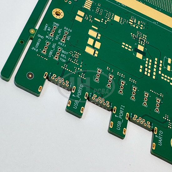
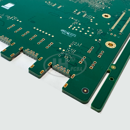
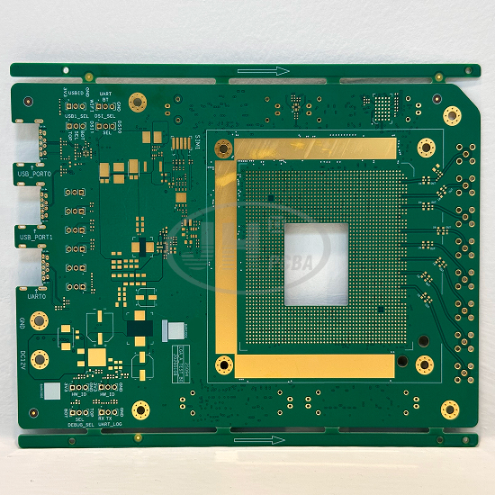
 Material: FR-4
Product Detail
10‑Layer High‑Layer‑Count Routing
Sufficient layer allocation enables separate power layers, ground layers and high‑speed signal layers to resist signal interference, supporting layout of high‑density large‑size BGA chips.
Halogen‑Free & Eco‑Friendly
Complies with automotive‑grade requirements and EU environmental regulations for export. Features V‑0 flame retardancy, excellent high‑temperature and humidity‑heat resistance.
Resin Via Plugging Process
BGA vias are fully planarized to avoid solder sinking and cold solder joints, improving assembly yield. It helps reduce board dimension and supports miniaturized design.
2 μm Thick Immersion Gold
Thick gold layer delivers great oxidation resistance, plug‑and‑play durability and superior conductivity. No gold peeling during multiple rework cycles, ideal for precise BGA soldering.
1.6 mm Standard Board Thickness
Balanced mechanical strength with good warpage resistance and high compatibility for mechanical assembly.
High Insulation Stability
Insulation resistance remains stable under temperature cycling and humid‑hot conditions, suitable for harsh working environments of automotive and industrial applications.
Custom Impedance Matching Available
Controlled‑impedance traces are supported to meet transmission requirements of high‑speed and high‑frequency signals.




