189-2464-6170
 szjhpcb@VIP.126.com


 Material: FR-4
Product Detail
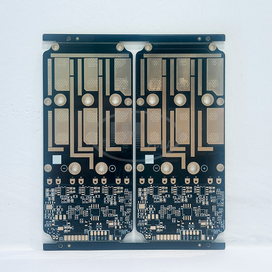
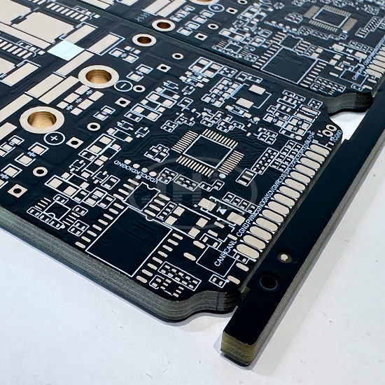
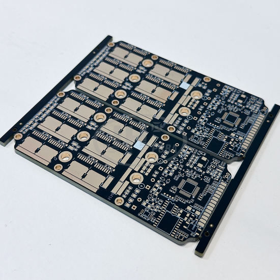
8-Layer 3.2mm Extra-Thick Multi-Layer Structure: Extremely high mechanical strength, vibration resistance and anti-bending deformation. Partitioned multi-layer power and ground planes deliver low voltage drop for high-power loops and excellent heat dissipation.
Heavy Copper Design: Increased copper thickness enables superior ultra-high current carrying capacity. Suitable for high-current charge & discharge and power circuit routing with low temperature rise and less heat generation.
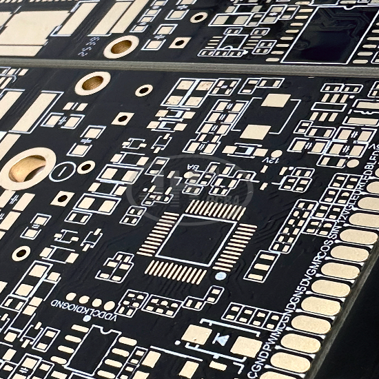
Conductive Copper Paste Plugged Via Process: Through holes filled and conducted with copper paste to realize vertical high-current interconnection between layers. It replaces traditional series vias with lower on-resistance and larger current capacity, and resolves space constraints of densely arranged vias.
2μ" ENIG Surface Finish: Pads feature oxidation and corrosion resistance, ensuring reliable soldering for MOSFETs and power chips. Hardly gold peeling after multiple reworks, ideal for SMT assembly of high-power components.
Stepwise Lamination Process for Thick Boards: Effectively releases internal board stress, eliminates common defects such as delamination, blistering and warpage of thick PCBs, and maintains stable dimensional performance during long-term operation under temperature variation.
Black Solder Mask with Large-Area Copper Pour: Higher heat dissipation efficiency, premium appearance, light shielding and anti-interference performance, applicable to densely-heated layout of power products.
High-Voltage Interlayer Isolation Design: Layer separation for strong and weak electricity with sufficient insulation margin, meeting safety design requirements of high-voltage and high-power circuits.