189-2464-6170
 szjhpcb@VIP.126.com

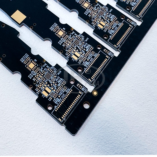
 Material: FR-4
Product Detail
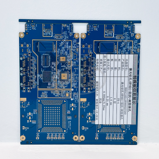
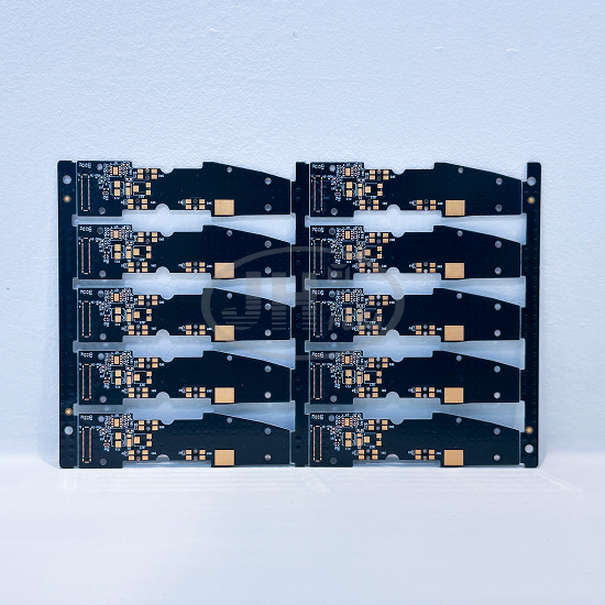
6 Layer 1-Stage HDI Buried Blind Via PCB | FR4 BGA Resin Plug Circuit Board for Communication
Product Introduction
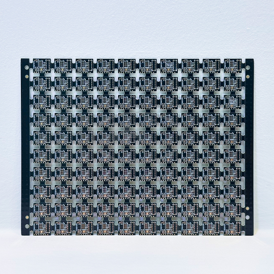
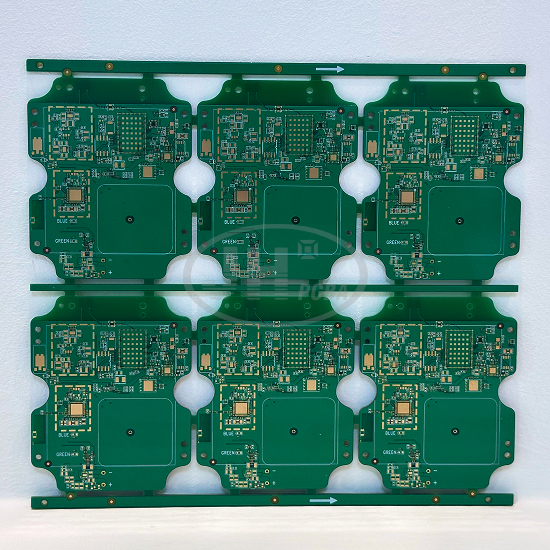
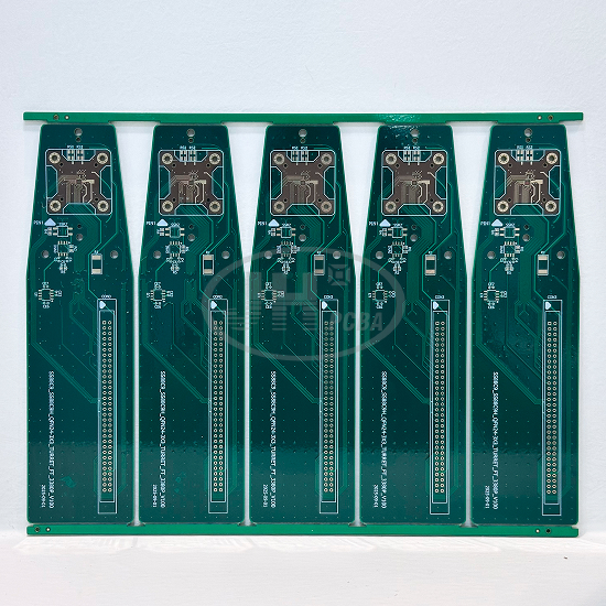
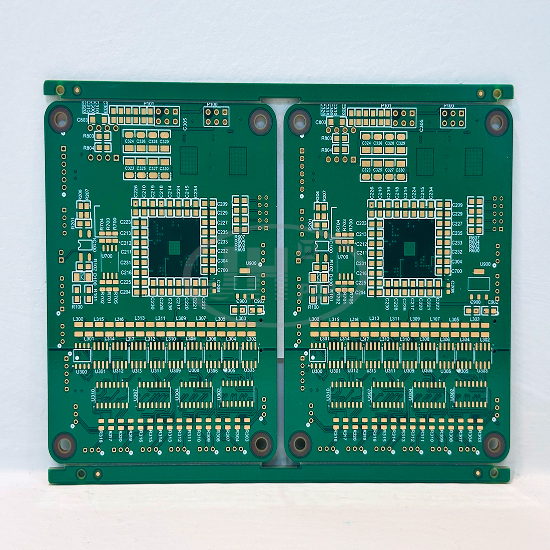
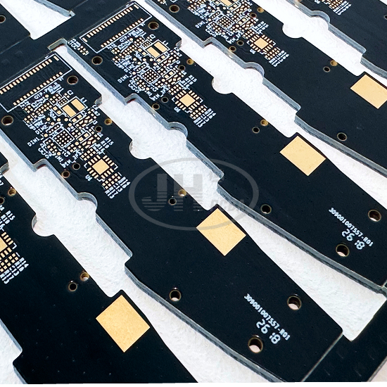
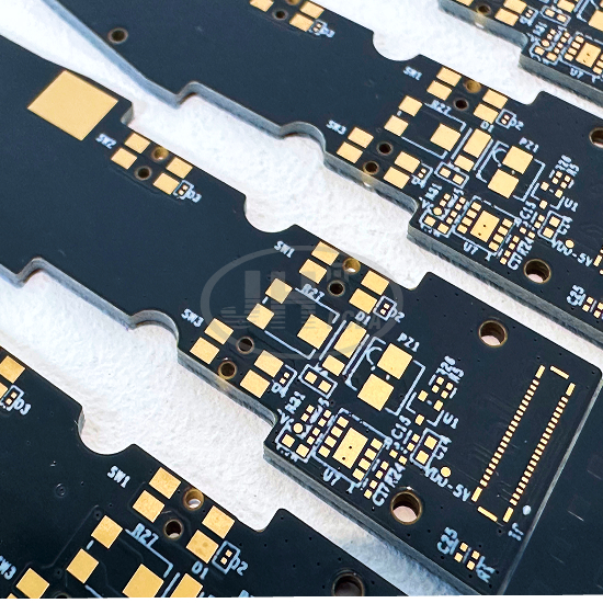
This high precision 6-layer 1-stage HDI PCB board is built on FR4 flame retardant substrate with finished thickness 0.8mm. It supports ultra-fine 3mil line width & space, laser micro blind via down to 0.075mm. Surface treatment is ENIG gold plating, equipped with BGA pad layout and resin plug technology, black solder mask, panel design for mass SMT assembly.
HDI buried blind via technology enables high density routing in limited board area, reduces signal attenuation and electromagnetic interference, perfect for modern compact high-speed communication electronics. Resin plug flattens the via holes to eliminate hidden solder risk, greatly enhance soldering stability for BGA packages, improve product service life in harsh working environment.
Product Specifications
PCB Layers : 6 Layers, 1 Stage HDI, Buried & Blind Vias
Base Material : FR-4, UL94 V-0, E-glass fiber reinforced epoxy resin
Finished Board Thickness : 0.8 mm
Minimum Via Diameter : 0.075mm Laser Micro Blind Via
Min Trace / Space : 3mil / 3mil
Surface Finish : ENIG (Electroless Nickel Immersion Gold)
Solder Mask Color : Black
Special Features : HDI buried blind via, BGA pad design, resin plug, stamp hole panelization
Application Field : Communication Equipment
Production Technology
- HDI 1-stage interconnection structure, blind vias by UV laser drilling, inner buried vias for interlayer connection, optimize high speed signal integrity.
- Resin plugging & grinding process: fully fill vias, planarize PCB surface, allow routing on plugged vias.
- LDI direct imaging process for consistent 3mil ultra-fine circuit, avoid line break and short circuit.
- ENIG gold finish provides outstanding oxidation resistance and stable soldering performance for BGA components.
Application Scenarios
5G modules, optical communication circuit boards, radio frequency control boards, mini base station PCB, communication gateway and high-speed signal transceiver hardware.
Why Choose Juehuiweiye Circuit?
We are a professional HDI PCB manufacturer in China, specializing in high-density HDI circuit board prototyping and volume manufacturing.
We are capable of complicated HDI technologies including microvia, ultra-fine line, resin plug and BGA PCB fabrication.
Our factory is equipped with full advanced machines, implement strict quality control, all boards pass 100% flying probe electrical test.
We offer free DFM analysis, fast turnaround for samples, flexible MOQ for small batch and mass order. Customization is welcome according to your drawing & requirements.
RoHS & UL compliant.
Order Information
Please send Gerber files, stack-up requirement, impedance specification and surface finish requirement for quotation and manufa
📞 Tel:+86 189-2464-6170
📧 Email:szjhpcb@vip.126.com
🌐 Official Website:https://www.szjhpcba.com/