189-2464-6170
 szjhpcb@VIP.126.com

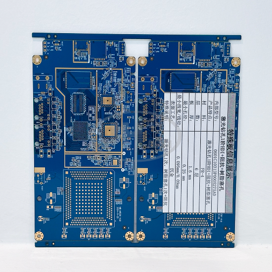
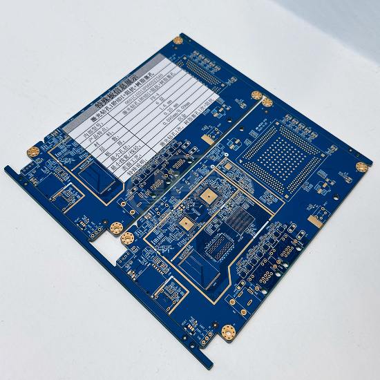
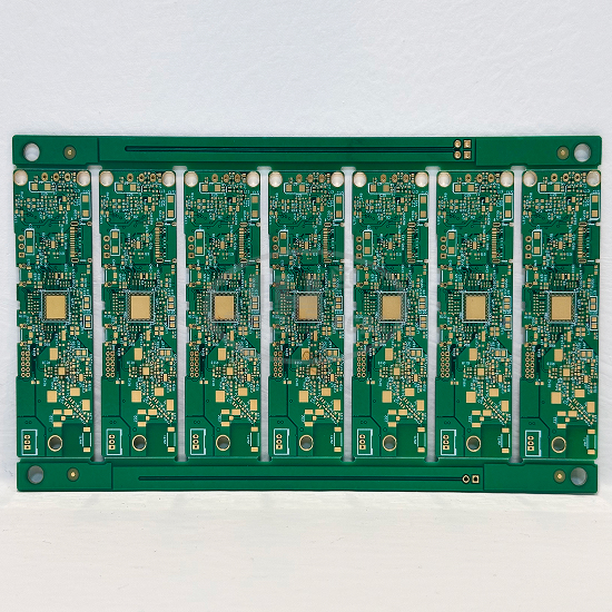
 Material: FR-4
Product Detail
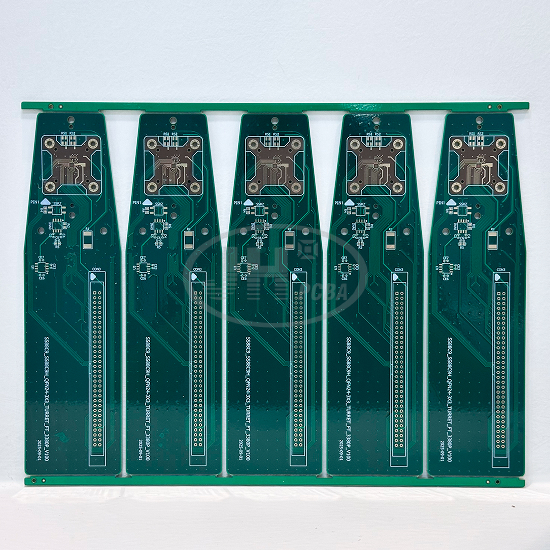
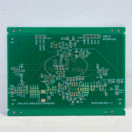
6-Layer 1-Stage HDI Structure for Significantly Higher Routing Density
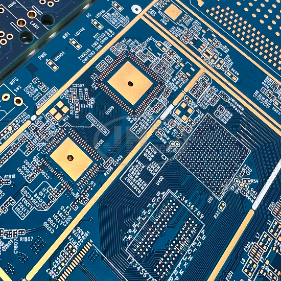
Laser blind vias connect the outer layer to the adjacent inner layer, freeing up inner-layer routing space. It accommodates high-pin-count dense BGAs and integrates Ethernet ports, RF circuits, DDR and multi-channel power circuits within standard board dimensions, supporting miniaturized design of communication equipment.
Enhanced Long-Term Reliability with Single Resin Plugging for Buried Vias
Buried vias are filled and planarized to prevent solder entrapment and bubbling during SMT assembly, offering moisture and corrosion resistance. Continuous multi-layer power and ground planes deliver low voltage drop under high current and excellent heat dissipation for stable long-duration continuous operation.
Full-Process Precision Controlled Impedance
Closed-loop control of trace width, copper thickness and dielectric thickness ensures outstanding high-speed differential signal integrity with reduced crosstalk, reflection and attenuation. It meets timing specifications for Gigabit Ethernet and high-speed serial buses and achieves superior noise immunity for RF circuits.
ENIG Process Optimized for Precision Soldering
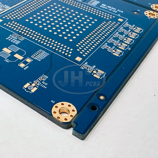
Flat BGA and fine-pitch pads feature oxidation and tarnish resistance with minimal discoloration after multiple reflow cycles. It provides far better stability for IC ball mounting and rework soldering compared with HASL.
Low Warpage via Stepwise Lamination for 6 Layers
Internal board stress is fully relieved to achieve superior surface flatness, compatible with high-precision mass assembly on high-speed SMT equipment and delivering high production yield.
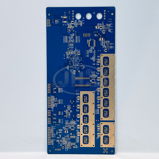
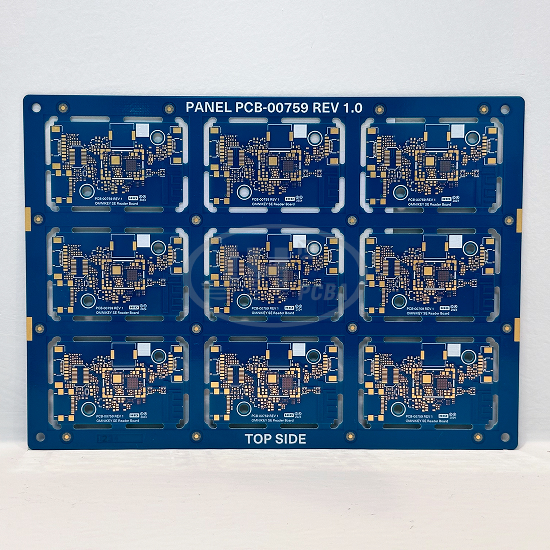
Blue Solder Mask & Communication-Specific Design
Blue solder mask provides high recognizability together with oil and aging resistance. Reserved layout for multi-channel Ethernet ports and isolated RF copper areas enables strong EMI suppression, suitable for network devices operating in complex electromagnetic environments.