189-2464-6170
 szjhpcb@VIP.126.com


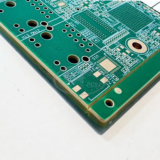
 Material: FR-4
Product Detail
I. 22‑Layer Ultra‑High‑Count 1+N HDI Stack‑up
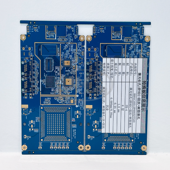
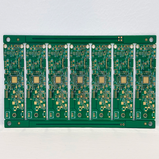
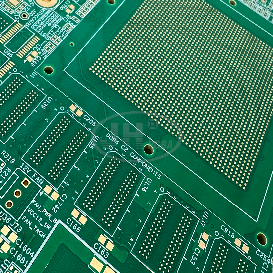
First‑order laser blind vias enable fast interconnection from outer layers to inner layers, greatly boosting routing density. It supports large‑pin‑count FPGA / BGA chips, accommodating numerous high‑speed differential and power networks within limited board space to meet design requirements of complex high‑speed computing circuits.
Differentiated Surface Finish on Two Sides
II. Immersion Gold for Component Area
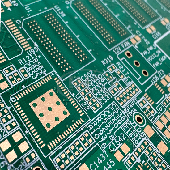
BGA pads feature flat surface with excellent anti‑oxidation and anti‑sulfidation performance. They resist discoloration after multiple reflow cycles and deliver outstanding reliability for ball‑mounting and precision chip soldering.
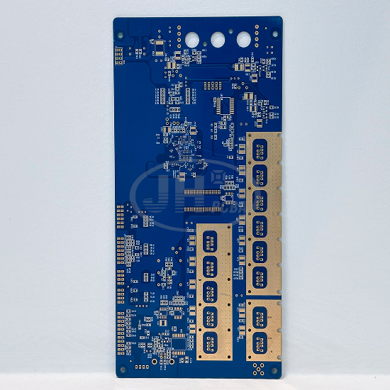
III. Electrodeposited Hard Gold for PCIe Gold Fingers
High hardness with great wear‑resistance and plug‑pull durability. Stable contact resistance under repeated long‑term mating, ensuring signal integrity for high‑speed bus.
IV. Closed‑Loop Precision Impedance Control Throughout Manufacturing
Full‑process control over trace width, copper thickness and dielectric thickness ensures outstanding impedance consistency for high‑speed differential signals. It reduces crosstalk, signal attenuation and reflection, satisfying strict timing requirements of high‑speed buses such as PCIe and DDR4.
V. Multi‑Step Lamination for Minimal Deformation
Segmented lamination is adopted for 22‑layer ultra‑high‑count boards to release internal stress. It mitigates common defects of ultra‑high‑layer boards including warpage, delamination and voids. Board flatness meets high‑precision placement requirements of high‑end SMT equipment.
VI. 2.8 mm Thick Board with Robust Mechanical Structure
High mechanical strength and bending resistance. Resists deformation for card‑edge installation, suitable for long‑term operation in industrial chassis and server slot applications.
VII. Ultra‑High‑Density Routing Capability
Designed with fine traces, micro‑vias and small pads. Integrates massive power and ground planes for effective EMI shielding and superior anti‑interference performance, ideal for complex high‑speed computing systems.