189-2464-6170
 szjhpcb@VIP.126.com

 Material: FR-4
Product Detail
8-Layer 2-Stage HDI PCB (0.8mm Ultra-thin ENIG Board)
Product Overview
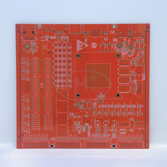
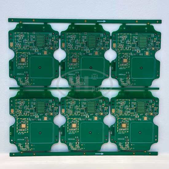
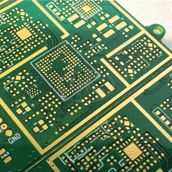
This is a precision 8-layer 2-stage HDI PCB from Juehui Weiye Circuit. Unit dimension: 115×116mm with a finished board thickness of only 0.8mm. It adopts core HDI technology including 2-stage blind & buried vias plus laser blind via filling. Solder mask is green, with ENIG surface finish.
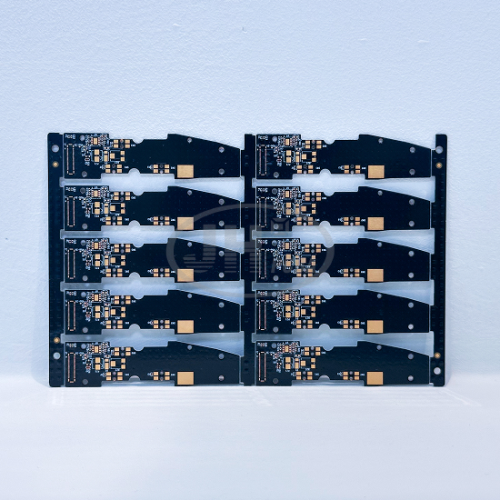
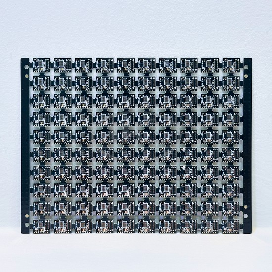
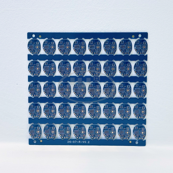
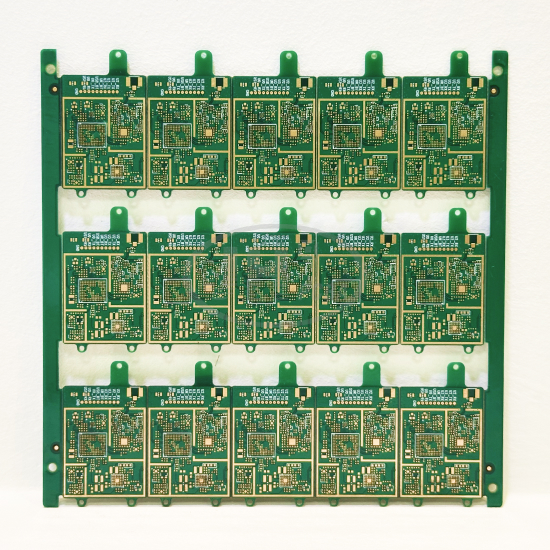
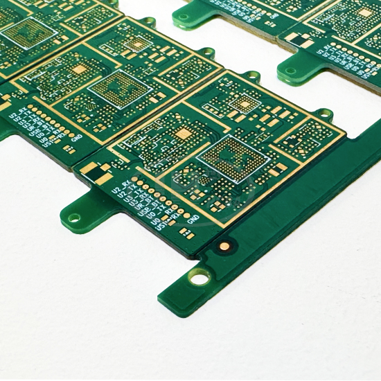
The panel is designed with tab-routing (stamp holes), pre-routed process edges and fiducial MARK points, compatible with automatic SMT assembly. Multiple BGA chips are integrated on the board with extensive blind-via fanout routing. Pins for USB, UART serial port and Bluetooth BT communication are reserved on the PCB, specially developed for IoT wireless communication main controllers.
It features an 8-layer stack-up with dedicated signal, power and ground layers. Differential impedance control is available to guarantee stable transmission of high-speed differential signals for USB and Bluetooth. The ultra-thin 0.8mm board imposes strict requirements on lamination, shrinkage & expansion and warpage control. The 2-stage HDI undergoes two rounds of laser drilling, two laminations and blind via electroplated filling to achieve ultra-high routing density, enabling multi-chip integration within a compact footprint.
Core Specifications
- Layers: 8 layers, 2-stage HDI (2nd-order blind & buried vias)
- Unit Size: 115×116 mm
- Finished Board Thickness: 0.8 mm
- Core Process: 2-stage laser blind vias, blind via plating filling, 3×5 panel array
- Solder Mask Color: Green solder mask, white legend
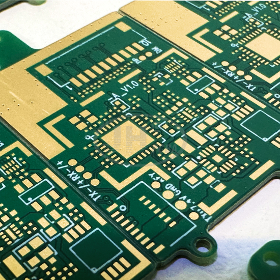
- Surface Finish: ENIG (Electroless Nickel Immersion Gold)
- Base Material: High-TG FR-4, TG≥170℃, UL94 V-0 flame retardant
- Minimum Laser Blind Via Diameter: 0.075 mm
- Minimum Mechanical Through Hole Diameter: 0.15 mm
- Minimum Trace Width / Space: 0.075 mm / 0.075 mm
- Copper Weight: Outer layer 1/3 oz, Inner layer 0.5 oz
- Optional Processes: Impedance control, resin via filling, alternative surface finishes
Product Advantages
1. 2-stage HDI blind & buried via structure with laser blind via filling, high-density BGA fanout, realizing multi-chip integration in compact size;
2. Ultra-thin 0.8mm board with dedicated lamination process. Board warpage and dimensional change are tightly controlled to suit automatic SMT mounting;
3. ENIG finish delivers flat and uniform BGA pads, excellent oxidation resistance, tolerance to multiple reflow cycles and high assembly yield;
4. Custom differential impedance supported, compatible with high-speed USB, Bluetooth and serial signals for superior signal integrity;
5. Panel array + fiducial MARK design for full-panel SMT production, easy depaneling and seamless adaptation to customer mass-production lines;
6. High-TG substrate prevents delamination after repeated lamination, ensuring reliable blind vias and stable long-term operation;
7. Full-process AOI + 100% flying probe electrical test, rigorous screening for fine-line defects to guarantee consistent quality.
Fabrication Flow (Standard 2-Stage HDI Process)
Material Cutting → Inner Layer Patterning → Inner AOI → 1st Lamination → Laser Drilling (1st-stage Blind Vias) → Blind Via Desmear → Blind Via Electroless Copper → Via-Fill Plating → Grinding → Outer Layer 1 Patterning → AOI → 2nd Lamination → Laser Drilling (2nd-stage Blind Vias) → Desmear → Electroless Copper → Via-Fill Plating → Grinding → Outer Layer Exposure & Etching → Outer AOI → Solder Mask (Green) → Legend Silk Screen → ENIG Plating → Routing & Stamp Hole Processing → Electrical Test → FQC Visual Inspection → Packaging & Shipment
>
> Key Note: 2-stage HDI requires two laser blind drilling cycles and two laminations with blind via plating filling. We strictly control board warpage, via dimple and voids. For the ultra-thin 0.8mm board, lamination pressure and temperature profile are monitored throughout the whole process to avoid thin board deformation.
Application Industries & Suitable Products
Industries: IoT, Wireless Communication, Smart Terminals, Portable Industrial Control, Bluetooth Communication Modules, High-Speed Signal Acquisition
Suitable Products: Bluetooth Main Controller Boards, USB Communication Control Boards, Portable Intelligent Acquisition Terminals, Wireless Sensor Motherboards, Compact IoT Gateways, Portable Testing Instruments, Wearable Main Boards, Micro Industrial Data Acquisition Boards.
Judging from silkscreen labels U2_RX/TX, USB and BT pins, this is an integrated main controller PCB supporting Bluetooth, UART serial and USB communication.
Certifications
All precision PCB products of Juehui Weiye Circuit comply with international standards and hold complete authoritative certifications, with traceable quality up to medical-grade requirements:
✅ ISO9001 Quality Management System: Standardized closed-loop production control for consistent product precision and performance;
✅ ISO13485 Medical Device Quality Management System: Compliant with quality specifications for medical supporting PCBs;
✅ UL Safety Certification: Qualified flame retardancy and insulation to meet international safety standards;
✅ RoHS Compliance: Lead-free and halogen-free, free of hazardous substances;
✅ REACH Compliance: Meets EU chemical regulations, supporting export to overseas markets.
Juehui Weiye Circuit PCB Customization Service
Juehui Weiye Circuit has stable mass-production capability for 8-layer 2-stage HDI PCBs. We accept prototype and small-to-medium batch orders for ultra-thin HDI, blind & buried vias, laser blind via filling and high-density BGA boards.
✅ Mature 2-stage HDI process, 0.075mm laser blind vias with fully filled vias free of voids or dimples;
✅ Dedicated lamination process for 0.8mm ultra-thin boards, tight control of warpage and dimensional shift for automatic SMT assembly;
✅ Custom impedance control for differential USB and serial signals to preserve high-speed signal integrity;
✅ ENIG finish with flat BGA pads and precise solder mask opening to avoid solder mask bridging on pads and improve SMT yield;
✅ Support stamp-hole panelization, process edge design and fiducial MARK points, matching customer SMT production lines. We are a professional Shenzhen PCBA manufacturer;
✅ Full-process AOI optical inspection + 100% flying probe electrical test to strictly screen open/short circuits on fine traces;
✅ Gerber review, impedance simulation and stack-up optimization available, with supporting documents for foreign trade orders;
✅ Multi-stage HDI and any-layer HDI available, resin via filling and optional surface finishes (ENIG / Hard Gold / Immersion Tin).
We specialize in custom high-density precision HDI PCBs, providing one-stop manufacturing for IoT wireless main controller boards and compact ultra-thin control boards with fast prototyping and controllable mass lead time.
Our one-stop services include stack-up evaluation, impedance simulation, CAM engineering optimization, laser blind via filling and panelization design. Multiple surface finishes such as ENIG, Immersion Tin and Hard Gold are available. We can review and quote based on your Gerber files, support documentation coordination for overseas orders. Feel free to send your files for inquiry.