189-2464-6170
 szjhpcb@VIP.126.com


 Material: FR-4
Product Detail
Ultra‑Thin 1‑Stage HDI Structure
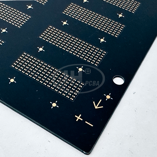
0.4 mm ultra‑thin board thickness combined with laser‑drilled 1‑stage blind vias greatly increases surface‑layer routing density. It is compatible with ultra‑high‑pin‑count chips and meets the constraints of lightweight and miniaturized end‑product designs.
High‑Reliability Blind & Buried Vias with Single‑Pass Resin Plugging
Buried vias are filled and planarized with resin to prevent bulging and solder trapping during SMT soldering. It delivers excellent moisture and corrosion resistance. Multi‑layer power and ground planes improve power‑supply stability for long‑duration continuous‑operation applications.
Precision Process for Ultra‑Fine Traces
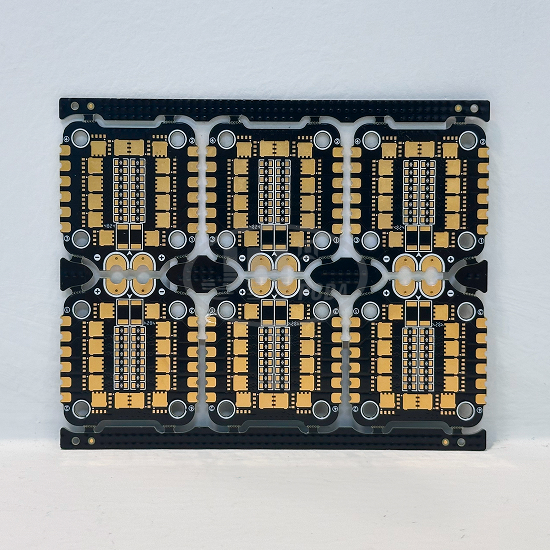
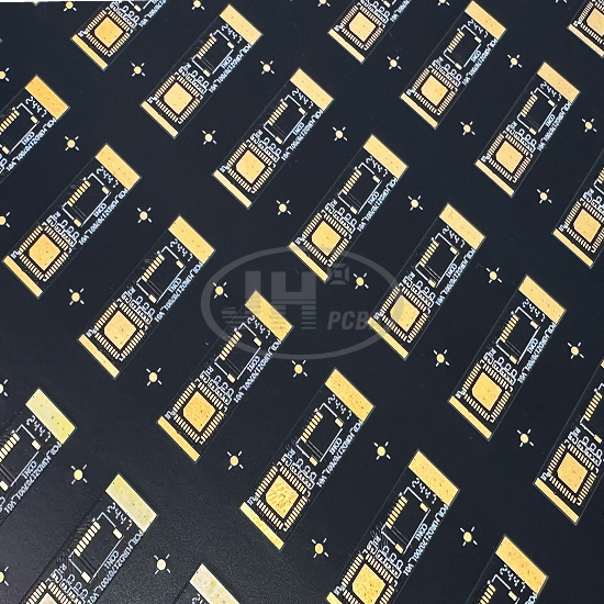
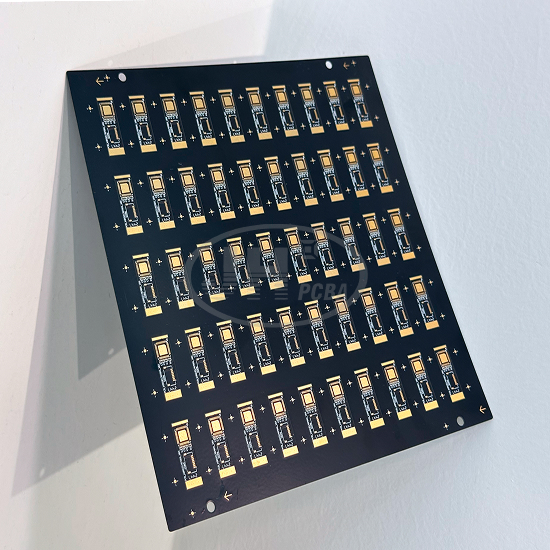
Minimum trace width / space: 0.105 mm / 0.088 mm; minimum hole size: 0.15 mm. Supports high‑density matrix panel layout for high panel yield and cost‑effective mass production.
Matte Black Solder Mask with Immersion Gold Surface Finish
Black solder mask blocks light and reduces reflection, ideal for optical‑recognition applications. Flat immersion‑gold‑finished pads resist oxidation, deliver high yield through multiple reflow cycles, and ensure reliable BGA ball‑mounting for fine‑pitch components.
Matrix Panelized Design for Volume Manufacturing
Neat multi‑unit panel layout optimized for high‑speed SMT assembly. Low stress during depaneling minimizes warpage and edge chipping, significantly boosting mass‑production yield.
Low‑Warpage Control for Ultra‑Thin Boards
Symmetric stack‑up plus step‑by‑step lamination relieves internal stress. Board flatness meets precision requirements of high‑speed placement machines, solving the common industry pain point of thin‑board warpage.