189-2464-6170
 szjhpcb@VIP.126.com


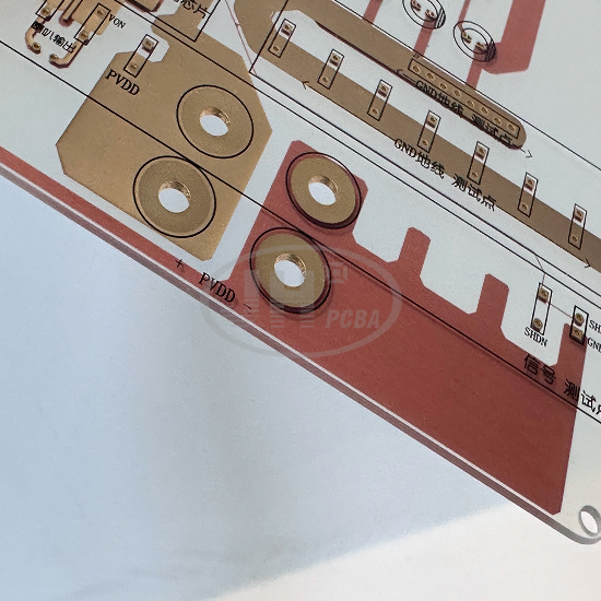
 Material: Available Substrate Materials
Product Detail
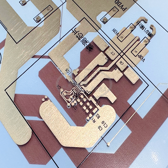
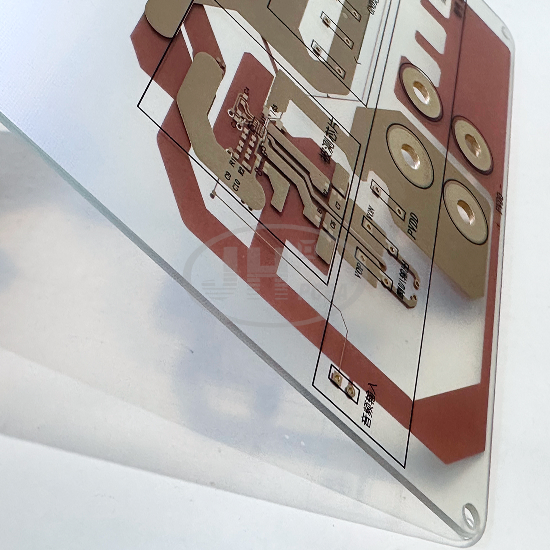
Full-Link Transparent Visualization: Dual light-transmitting design with transparent substrate and transparent solder mask. Internal copper traces and routing paths are fully visible, facilitating debugging & troubleshooting, teaching demonstration and process verification.
High Reliability via Resin Plugged Vias: Vias are completely filled and planarized with resin. No solder trapping or bubbling under high-current operation. Excellent moisture and corrosion resistance greatly extends the service life of repeatedly used test boards.
Durable ENIG Test Contacts: Test pads are gold-plated to withstand hundreds of thousands of repeated probe touches. Contact resistance remains stable without oxidation or darkening.
1.0mm Standard Ultra-Thin Thickness: Moderate rigidity resists deformation, suitable for mounting and fixing on test fixtures. Wide copper traces support high-power power input.
Traceable Materials with Certificates: Original material reports, RoHS and flame retardant certifications are available for substrates, solder mask and resin, meeting laboratory compliance requirements.
Balanced Insulation & Optical Performance: Retains excellent electrical insulation of PCBs while achieving high light transmittance for demonstration purposes, breaking the visual limitations of traditional green solder mask PCBs.