189-2464-6170
 szjhpcb@VIP.126.com



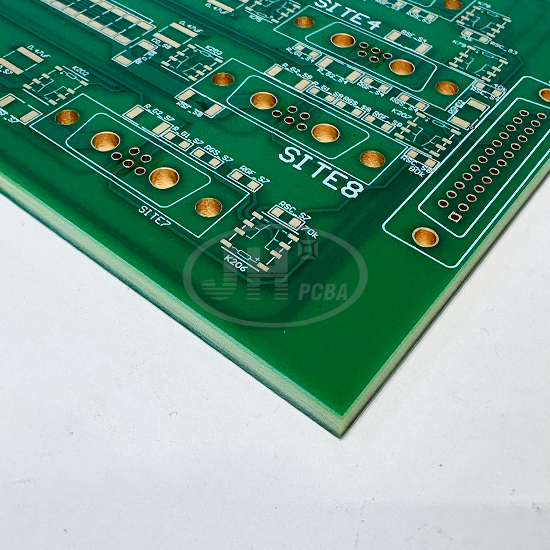
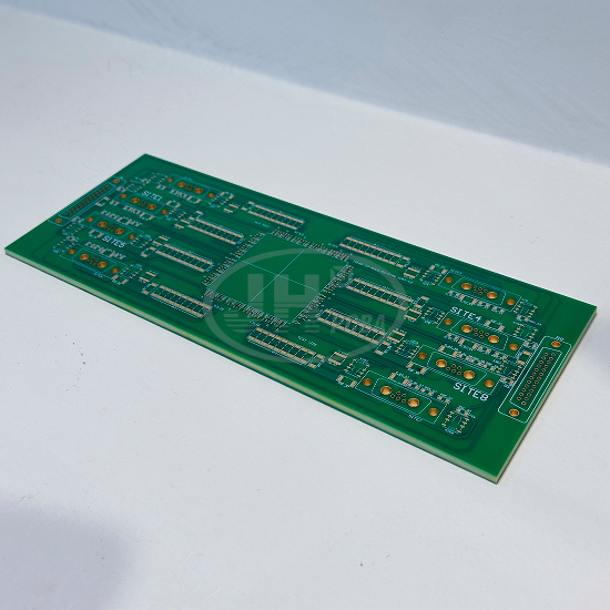
 Material: FR-4
Product Detail
3.2mm Extra-Thick Multilayer Structure
Extreme mechanical rigidity with excellent resistance to vibration, bending and deformation. It delivers outstanding high-current carrying capacity and thermal dissipation, and maintains stable shape under repeated fixture pressing.
0.5mm Precision Small Slot Technology
High forming accuracy for narrow slots with smooth slot walls and reliable insulation. It meets design requirements for structural clearance, strong/weak current isolation and routing area partitioning.
2μ" ENIG Surface Finish
Contact pads feature oxidation resistance, wear resistance and durability against repeated mating. Gold layer is not prone to peeling under repeated probe testing, ensuring reliable SMT soldering on miniature pads.
Step Lamination Stress Relief Design
Effectively eliminates common defects of thick PCBs including delamination, voids and warpage, and guarantees stable dimensional performance during long-term operation under temperature variation.
Multi-Station Partitioned Routing
Independent shielding for multiple test channels prevents signal crosstalk and delivers high testing accuracy, suitable for synchronous mass-production testing at multiple stations.
High-Voltage Withstand Insulation Design
Customizable high-voltage isolation structure between layers, compatible with mixed high/low voltage test circuits and providing sufficient safety margin.
High-Wear Contact Design
Optimized for frequent probe contact testing, offering far longer service life compared with HASL circuit boards.