189-2464-6170
 szjhpcb@VIP.126.com

 Process Steps: PCB Fabrication + Precision SMT Mounting + DIP Through-hole Assembly + Manual Soldering + Inspection
Case Detail
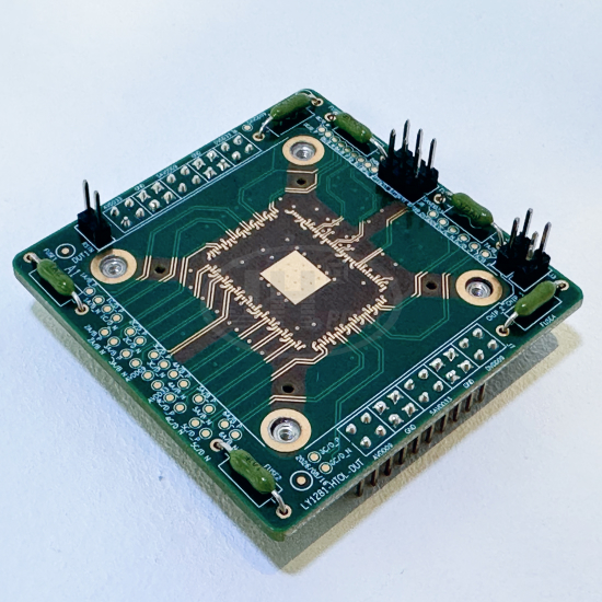
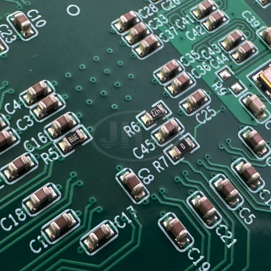
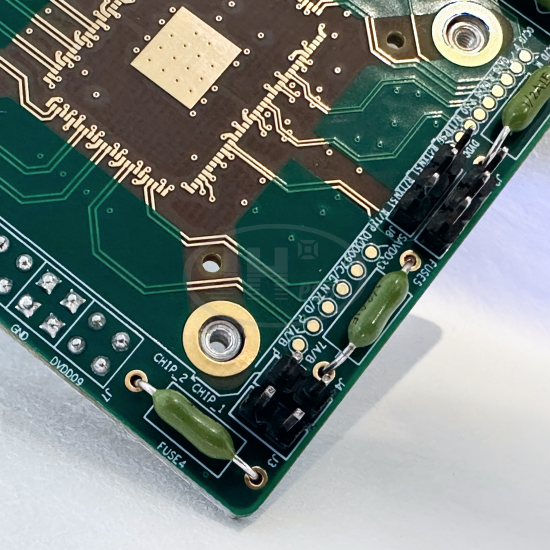
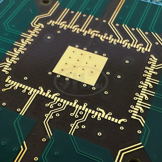
This BGA chip test fixture PCBA has a finished dimension of 55mm×55mm. It is a square double-sided test carrier board with one-stop manufacturing service including PCB fabrication, SMT mounting, DIP insertion and manual soldering. A dedicated BGA chip mounting area is reserved at the board center. It serves as a dedicated fixture board for DUT functional verification and electrical performance testing of chips.
Equipped with resistors & capacitors, fuses, through-hole pin headers and PEM self-clinching nuts, the board can quickly connect with test jigs to realize chip power supply, signal routing and functional detection. It is suitable for pre-production sample validation and mass-production ATE testing of chips.
Juehui Weiye Circuit undertakes custom manufacturing of high-complexity BGA carrier PCB and PCBA, supporting X-Ray inspection and precision SMT assembly for BGA boards.
1. Basic Specifications
PCBA Finished Size: 55mm × 55mm
PCB Material: FR-4 6-layer board (BGA carrier board), high-TG material
Board Thickness: 1.6mm
PCB Surface Finish: ENIG (Electroless Nickel Immersion Gold)
Minimum Trace Width / Spacing: 0.075mm / 0.075mm
Minimum Hole Size: 0.1mm (BGA via)
Core Packages: BGA (socket for DUT chip), 0402 SMT resistors & capacitors
Minimum Pin Pitch: 0.5mm for BGA
Total Solder Joints: approx. 1420 joints (including BGA zone, SMT component joints and DIP solder joints)
2. BOM & Component Function Description
1. SMT Capacitor (0402)
Function: Power supply filtering and voltage stabilization. Suppress power ripples, provide local energy storage for each power pin of the BGA chip to ensure stable power supply.
2. SMT Resistor (0402)
Function: Current limiting, voltage division, pull-up/pull-down for signals, match signal impedance and set circuit operating conditions.
3. SMT Crystal Oscillator Y1
Function: Generate reference clock signal and provide timing reference for the test circuit.
4. Glass Glaze Fuse Resistor (Green Through-hole Fuse)
Function: Over-current protection for multi-channel power circuits, preventing test equipment and fixture board burnout in case of short circuit of DUT chips.
5. DIP Pin Header
Function: External interface for power and signal routing, connecting with test machines to transmit power, IO and communication signals.
6. PEM Self-clinching Nut (M2×4)
Function: Fixture mounting hardware, used to fasten the PCBA onto the base of test jigs.
7. BGA Pad Area (Bare pads for DUT chip)
Function: Mounting zone for DUT BGA chips, routing all signal pins of the chip to peripheral circuits.
> Total Component Categories: 6 types; Total Component Quantity: 71pcs
3. Manufacturing Process
Process Flow: PCB Fabrication + Precision SMT Mounting + DIP Through-hole Assembly + Manual Soldering + Inspection
1. PCB Fabrication: Production of 6-layer BGA carrier board with micro buried & blind via technology and ENIG surface finish to guarantee flatness and solderability of BGA pads.
2. SMT Assembly: 10-zone lead-free reflow soldering for mounting 0402 resistors, capacitors and crystal oscillator; bare pads reserved for BGA region.
3. DIP Insertion: Assembly of pin headers and fuse resistors.
4. Manual Post Soldering: Soldering and reinforcement for fuse resistors.
5. Quality Inspection: AOI optical inspection + X-Ray inspection (for BGA area to check voids and cold solder joints) + continuity test.
4. PCBA Application Fields
1. Semiconductor Chip Testing: DUT carrier board for sample verification, functional test and burn-in test of BGA packaged chips.
2. Chip R&D Laboratories: Pre-evaluation, scheme verification and debugging fixture for new chips.
3. ATE Automatic Test Equipment: Fixture board for chip mass production testing.
4. Embedded Solution Companies: Hardware debugging carrier board for processors and SOC chips.
5. Service Advantages of Juehui Weiye Circuit
Juehui Weiye Circuit has 11 years of experience in one-stop custom high-complexity PCBA manufacturing, specializing in BGA carrier boards and precision test fixture PCBA.
✅ Precision micro-pitch BGA mounting available, equipped with X-Ray inspection for BGA solder joint quality.
✅ One-stop delivery including high-layer PCB fabrication, SMT, DIP, post soldering and testing.
✅ Support quick prototyping for small batches and medium-volume mass production.
✅ Custom B2B service for industrial control, semiconductor testing, medical, security and other industries.
The company has obtained ISO9001 and ISO13485 medical-grade quality management system certifications. All products comply with international environmental standards including REACH, RoHS and UL.
We can meet your demands for rapid small-batch prototyping, medium-batch trial production and mass production. Customizable PCB layer count, board thickness, surface finish, impedance design and full test solutions.
Equipment manufacturers and solution companies in industrial control, medical, automotive, new energy, AI smart hardware, security, IoT and communication industries are welcome to send drawings, BOM and centroid files for sample consultation.
Order Instructions
Please provide PCB Gerber files, BOM list, centroid files and test specifications. We offer one-stop quotation and production evaluation covering PCB manufacturing, precision BGA SMT, DIP assembly, post soldering and firmware programming.
Board material, thickness, PCB layers, surface finish and component selection are all customizable.
📞 Tel: +86 189-2464-6170
📧 Email: szjhpcb@vip.126.com
🌐 Website: https://www.szjhpcba.com/