189-2464-6170
 szjhpcb@VIP.126.com

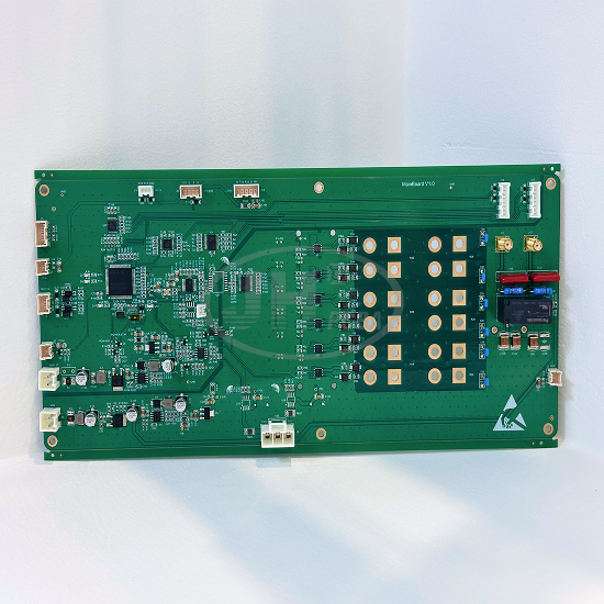
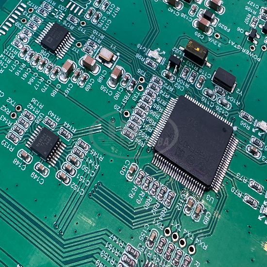
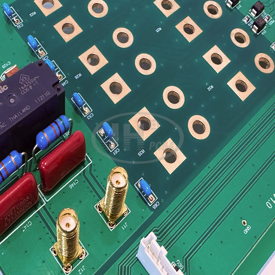
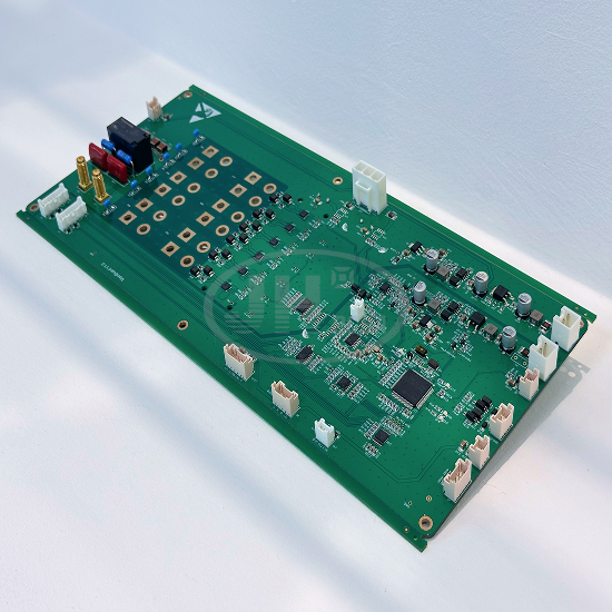
 Process Steps: Double-sided SMT + DIP Through-hole Components, Lead-free Reflow Soldering + Wave Soldering
Case Detail
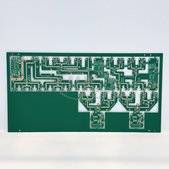
This MFUS MainBoard V1.0 is a high-power main control PCBA for medical devices, with finished dimensions of 312*147mm. It adopts FR-4 multilayer PCB substrate, board thickness 1.6mm, gold immersion surface finish, minimum trace width & spacing 0.12mm/0.12mm, and minimum hole diameter 0.25mm.
The board integrates main control MCU, power MOSFETs, high-voltage relays, large-capacity electrolytic capacitors and signal conditioning chips. It is equipped with SMA RF signal ports, multi-channel white terminal connectors and high-power pad arrays. Functions include high-power power conversion, multi-channel signal acquisition, relay switching control, RF signal access and peripheral communication driving.
Manufactured by double-sided SMT + DIP assembly with lead-free reflow & wave soldering. Components are placed in zoning layout with separation of strong and weak electricity, delivering outstanding anti-interference performance and high-power load driving capability. It is designed to match complete large medical ultrasound equipment.
Juehui Weiye Circuit has mature manufacturing capability for high-power medical equipment PCBA. We provide one-stop customized processing services including PCB fabrication, SMT mounting, DIP insertion and full-set FCT functional test. Board revision iteration is supported, covering low-volume prototype trial production through mass delivery.
Basic Parameters
1. Model: MFUS MainBoard V1.0
2. PCB Size: 312*147mm
3. PCB Layers: 4 Layers
4. Substrate: FR-4 High TG Material
5. Board Thickness: 1.6mm
6. Surface Finish: Immersion Gold
7. Min Trace Width / Spacing: 0.12mm/0.12mm
8. Min Hole Diameter: 0.25mm
9. Soldering Process: Double-sided SMT + DIP, Lead-free Reflow + Lead-free Wave Soldering
10. Power Input: Supports high-voltage DC input; on-board multi-channel voltage regulator circuits for multiple voltage outputs
11. Core Components: 32-bit Main MCU, Power MOSFETs, Signal Op-Amps, Optocouplers, Panasonic High-power Relays, High-voltage Film Capacitors, Large-capacity Electrolytic Capacitors, SMA RF Connectors
12. Interface Resources: SMA RF Signal Port, Multi-channel Peripheral Communication Terminals, Power Output Pad Array, Sensor Acquisition Port, Programming Port, High-power Terminal Block
13. Component Count
- SMT Components: total 246 pads including resistors, capacitors, MOSFETs, main MCU, op-amps, optocouplers
- DIP Components: 22 through-hole parts including electrolytic capacitors, high-voltage film capacitors, power relays, SMA RF connectors
- Min Package: 0402
- Min Pin Pitch: 0.5mm
14. Compliance: RoHS compliant. 100% power-on FCT functional test and high-voltage insulation test before shipment
Manufacturing Process
1. PCB Fabrication: Cutting → Drilling → Copper Plating → Inner Layer Patterning → Lamination → Outer Layer Patterning → Etching → Solder Mask → Silkscreen → Immersion Gold → Routing → Continuity Test
2. PCBA Assembly
Board Loading → Solder Paste Printing → SPI Inspection → Double-sided Mounting → Reflow Soldering → AOI Optical Inspection
DIP Insertion → Lead-free Wave Soldering → Cleaning → Manual Visual Inspection + AOI Recheck → FCT Power-on Functional Test & Withstand Voltage / Insulation Test → Final Cleaning → Packing & Shipment
3. Process Features: Zoned routing for strong & weak electricity; safety creepage distance reserved for high-voltage zones. Stable placement of 0402 micro packages. Wave soldering for high-power through-hole parts to guarantee high-current reliability. Multiple inspection stages across the whole workflow to avoid cold joints, short circuits and misplacement, satisfying stability requirements for long-term continuous operation under high-voltage complex working conditions.
Application
MFUS MainBoard V1.0 is a main control drive board, categorized as high-power medical control board. It is mainly applied in Class III medical high-power complete equipment and integrated ultrasound system (main unit + handpiece). It undertakes RF signal sampling, high-power load switching control, multi-channel sensor data acquisition and peripheral communication interaction, realizing overall logic control, high-voltage circuit protection and parameter collection.
Target Industries: Medical Devices, Aesthetic Medical Equipment, Large Laboratory Test Platforms and other high-end B2B equipment manufacturing sectors.
Advantages of Juehui Weiye Circuit PCBA Custom Service
Juehui Weiye Circuit specializes in one-stop customized PCB & PCBA manufacturing, certified to ISO13485 (Medical) and ISO9001 quality management systems. We undertake custom projects of high-power industrial control boards, signal acquisition boards and power drive boards.
✅ Accept BOM + Gerber from clients; schematic-to-PCB design and hardware revision available
✅ Support low-volume prototype trial & mass production with fast sampling lead time
✅ Full-process quality control: PCB self-inspection, SMT/AOI, FCT, withstand voltage & insulation test. MES traceability, customized test solutions on request
✅ RoHS lead-free process; samples and factory test reports available
✅ Two cooperation modes: component sourcing by us or customer-supplied components
Medical device manufacturers and instrument R&D companies are welcome to inquire for PCBA sampling and mass OEM, customized hardware solutions available upon demand.
Ordering Instructions
Please provide PCB Gerber, BOM list, centroid files and functional test specification. We will deliver quotation and production evaluation for PCB fabrication, SMT and through-hole assembly. Board material, layer count, surface finish and component sourcing plan can be adjusted as required.
📞 Tel: +86 189-2464-6170
📧 Email: szjhpcb@vip.126.com
🌐 Website:https://www.szjhpcba.com