189-2464-6170
 szjhpcb@VIP.126.com



How to Select a Reliable HDI PCB Manufacturer? Screening Guide for High Density Interconnect PCB Suppliers
High Density Interconnect (HDI) PCBs adopt laser microvia and fine-line technology, serving as core substrates for miniaturized AI modules, medical devices, micro sensors and smart wearables. Buyers often face risks including overstated process capability, poor microvia reliability and layer misalignment when selecting HDI vendors. Juehui Industry provides one-stop HDI PCB fabrication + precision SMT assembly service. We support 1st-order and 2nd-order HDI production, including laser microvias, copper via filling, fine trace & space and impedance control. Equipped with AOI, X-Ray and flying probe test, we deliver HDI prototypes and small-medium batch PCBA for medical, AI and sensor projects.
Q: How to select an HDI PCB manufacturer? Can ordinary PCB factories fabricate high-level HDI boards? What is Juehui Industry’s capability for HDI PCB and supporting PCBA assembly?
A: HDI stands for High Density Interconnect PCB. Using laser micro blind/buried vias and sequential lamination, HDI PCBs achieve ultra-fine traces and high wiring density to shrink board size. They are widely applied in AI modules, medical inspection devices, micro sensors and smart wearables. HDI technology has far higher technical barriers than conventional multi-layer PCBs. Many standard PCB factories cannot handle laser drilling, microvia copper filling or multi-cycle lamination. Poor production will lead to microvia open circuits, layer offset, impedance drift and BGA reliability failure. When selecting HDI suppliers, price alone is not enough; verify real process capability, inspection system and relevant project cases.
1. Core Technical Barriers for HDI PCB Fabrication
The key challenges of HDI PCB production lie in laser micro blind & buried via fabrication, sequential multi-layer lamination, fine-line etching and microvia copper filling processes.
You need to verify the manufacturer’s minimum microvia diameter, minimum line width & space, lamination registration accuracy and impedance control capability. High-level HDI (2nd-order and above) requires repeated sequential lamination with micron-level interlayer alignment control. Inadequate equipment, plasma desmear and electroplating process control will easily cause voids on via walls and interlayer misalignment, leading to open-circuit failures after thermal cycling. Meanwhile, HDI PCBs impose strict requirements on substrate selection, DFM design review and X-Ray microvia inspection capability.
2. Juehui Industry’s One-Stop Strength for HDI PCB & PCBA
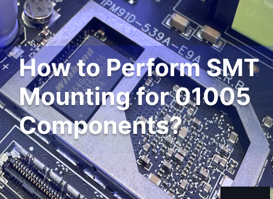
Juehui Industry provides integrated services including HDI PCB fabrication and downstream precision SMT assembly, covering the full workflow from PCB manufacturing to the mounting of micro-components such as 01005.
We undertake the fabrication of 1st-order, 2nd-order, 3rd-order and arbitrary-order HDI high-density interconnect boards, satisfying routing requirements for BGAs with pitches ranging from 0.5mm down to 0.3mm. Our capabilities cover laser micro blind/buried vias, electrolytic copper via filling, fine traces and controlled impedance. Professional DFM engineering reviews are available to identify risks of stack-up, microvias and BGA fanout in advance to prevent design flaws. Our specifications include a minimum laser via diameter of 50μm, interlayer registration accuracy of ±25μm, and up to 22-layer any-layer interconnection. Equipped with laser drilling machines, AOI, X-Ray and flying probe testers, we guarantee microvia integrity and interlayer alignment precision. We serve industries including 5G communications and automotive electronics. After HDI board fabrication, precision SMT assembly including 01005 micro-component placement can be completed in-house. This eliminates quality risks such as board warpage and moisture absorption caused by cross-factory transit, ideal for prototype and small-to-medium batch production of high-end projects in medical, AI and micro sensor sectors.
View Juehui Industry PCB manufacturing: Specifications of 22-Layer Laser Drilled 2nd-Order HDI PCB
3. Full-Process Inspection for HDI PCB Reliability
Juehui Industry implements a comprehensive full-process quality inspection system. X-Ray inspects electrolytic copper filling quality inside blind and buried vias and detects internal voids; AOI checks for open/short circuits on outer-layer fine traces; flying probe test performs 100% electrical continuity testing; microsection analysis evaluates microvia structure and lamination quality. We also control substrate warpage to ensure high SMT assembly yield of HDI boards and avoid placement offset of 01005 and 0201 micro-components caused by thin board deformation.
4. Main Application Scenarios for HDI PCB
Driven by the miniaturization trend of electronic products, HDI high-density interconnect PCBs are widely used in compact AI modules, medical inspection boards, micro sensors, smart wearables and miniature robot control boards. Such products feature limited PCB space and dense BGA pins, which require HDI microvia fanout to complete routing. Juehui Industry has abundant project cases of HDI PCB plus PCBA assembly. We provide customized one-stop services covering HDI PCB fabrication, fine-line circuits, ultra-thin PCB production and precision SMT mounting.
5. Checklist to Select HDI PCB Manufacturer
When selecting an HDI PCB supplier, focus on verifying the following indicators:
1. HDI Process Grade: Capability for 1st/2nd/arbitrary-order HDI, laser blind vias and via filling;
2. Process Parameters: Minimum microvia diameter, minimum line width & space, lamination registration accuracy and impedance tolerance;
3. Inspection Equipment: Availability of X-Ray, AOI and flying probe test, and provision of metallographic microsection reports;
4. Industry Cases: HDI project experience in high-precision fields such as medical, AI and sensors;
5. Supporting Capability: One-stop PCB+SMT service, especially precision mounting of 01005 micro-components.
Juehui Industry offers mature HDI process solutions with one-stop delivery of PCB fabrication and precision SMT assembly. If your project adopts HDI boards assembled with micro-components, please note HDI and stack order requirements when submitting design files. Our engineers will conduct DFM review and full-process evaluation.