189-2464-6170
 szjhpcb@VIP.126.com



How to Prevent PCB Warpage During Reflow Soldering? 10 Key Measures & IPC Acceptance Criteria
PCB warpage during reflow soldering is one of the most common defects in electronics manufacturing. Mild warpage impairs SMT placement accuracy and soldering quality, while severe cases can lead to full batch rejection. Fundamentally, board warpage arises from material mismatch under thermal stress: laminates, copper foils and solder mask expand and contract at different rates during heating and cooling. Combined with the board’s own weight and structural flaws in panelization, permanent deformation will occur. This article summarizes 10 major preventive measures and IPC acceptance criteria from three dimensions: design, laminate material and manufacturing process, for reference by engineers and procurement specialists.
1. Optimize Reflow Temperature Profile to Reduce Thermal Stress
Temperature is the primary source of board stress. On the premise of guaranteed soldering quality, appropriately lower the peak reflow temperature and slow down the heating-up and cooling rates to significantly mitigate board warpage.
Common engineering control parameters: heating slope of roughly 1.5~2°C/s to prevent glass fiber delamination caused by thermal shock; cooling rate in the cooling zone shall not exceed 4°C/s. Gentle cooling helps minimize residual laminate stress.
Where available, adopt a tent-style profile: Heat – Soak – Reflow – Slow Cool. Calibrate with thermal test boards for actual measurement, rather than directly applying generic profiles.
2. Select High-Tg, Low-CTE Laminate Materials
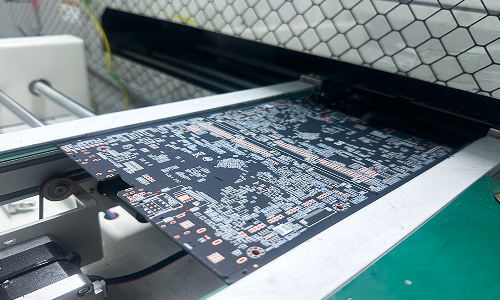
Tg refers to glass transition temperature. The lower the Tg value, the sooner and longer the laminate softens during reflow, leading to more severe deformation.
For lead-free reflow, laminates with Tg ≥150°C are recommended. For high-reliability products such as automotive electronics, choose Tg ≥170°C.
Also pay attention to CTE (coefficient of thermal expansion). A high Tg does not automatically mean low CTE. Materials with low Z-axis thermal expansion further suppress delamination and warpage. Both indicators shall be comprehensively evaluated during material selection.
3. Increase Board Thickness if Thin & Light Weight Is Not Mandatory
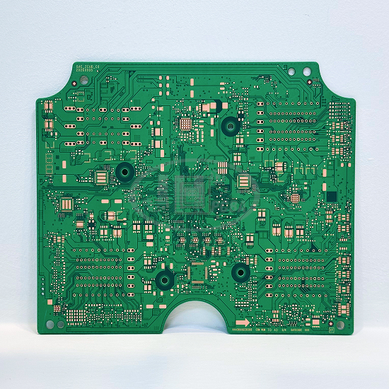
Many products adopt thin boards down to 1.0 mm, 0.8 mm or even 0.6 mm to achieve miniaturization. Such thin substrates are inherently difficult to remain undeformed through reflow. If lightweighting is not a hard requirement, a board thickness of 1.6 mm is strongly recommended to greatly reduce warpage risk. For thin-board designs, compensation measures such as reflow carriers and symmetrical stack-up are mandatory.
4. Adopt Strictly Symmetrical Stack-up Design
Symmetrical stack-up is the most effective method to reduce Z-axis stress at the design source. For multi-layer PCBs, copper distribution (thickness, area and location) shall be mirror-symmetrical relative to the central layer. Material properties, copper weight and pattern coverage of mirrored layers should be kept consistent.
A typical bad example: large copper pours only on one side of a single-sided board, or a 6-layer board with 2oz power layers paired with 0.5oz signal layers. Such asymmetrical stack-ups will inevitably warp under thermal stress.
5. Balance Copper Pouring; Avoid Large Copper Areas on a Single Side
Copper foil and substrate feature a large difference in CTE. Uneven copper distribution causes unbalanced thermal stress. If the top layer copper coverage reaches 80% while the bottom layer is only 20%, the board will bend like a stretched bow.
Control the copper coverage difference between two sides (or symmetric layer pairs) within 15%~20%. Add dummy copper blocks or grid copper in blank areas to balance stress and improve heat dissipation.
6. Control Panel Size; Align Narrow Edge Perpendicular to Conveyor Direction
Most reflow ovens use chain conveyance. Larger panels tend to sag under their own weight. Place the long edge of the PCB on the conveyor chain, with the narrow edge perpendicular to the oven travel direction to reduce gravity-induced sagging. Meanwhile, control panel dimensions (empirically, single panels better within 200 mm) and reduce panel count, which effectively improves reflow deformation.
7. Optimize Panelization Connection; Minimize V-Cut Usage
V-Cut weakens the structural integrity of panels. Use mouse bites (breakaway tabs) instead wherever possible, with tab width ≥2 mm. If V-Cut is unavoidable, reduce groove depth and reserve a minimum 0.5 mm copper-free zone on both sides of the V-Cut line to avoid stress concentration. For depaneling, prefer router routing over V-Cut separation to prevent warpage triggered by concentrated stress.
8. Add Process Edges and Stiffeners
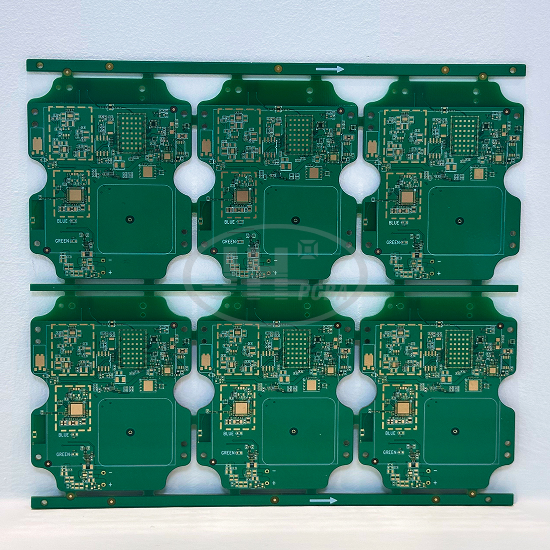
For large-size or multi-up panels, add process borders (≥5 mm recommended) and support bars along edges. Add copper stiffeners at PCB edges or underneath large components, or locally thicken board edges (e.g. 1.6 mm edge thickness with 1.0 mm inner area). This structurally boosts board rigidity and suppresses sagging and twisting during reflow.
9. Use Reflow Carrier Fixtures
When the above measures cannot meet requirements, reflow carriers offer the most direct solution. The fixture holds the PCB fixed through thermal expansion and contraction until the board cools below Tg and regains rigidity to retain original dimensions. If a single-sided carrier is insufficient, add a top cover to clamp the PCB from both sides for dramatic deformation reduction. The downside is higher fixture cost and manual loading/unloading work.
10. Pre-Bake for Moisture Removal & Process Control
Moisture absorption in laminates worsens delamination and warpage during reflow. Prior to production, bake PCBs at approximately 120°C for 2~4 hours according to thickness to remove absorbed moisture. Use thermal test boards to measure and record actual reflow profiles, fine-tuning parameters based on board thickness and component density. Maintain oven cleanliness and uniform hot air flow to prevent amplified deformation from local temperature difference.
Acceptance Criteria for PCB Warpage
Per relevant IPC standards: the maximum allowable deflection for PCBs with SMD components is 0.75% of board length; for PCBs without surface-mount devices, the limit is 1.5%.
For high-reliability products such as automotive and medical electronics, internal specifications are usually stricter (some high-grade requirements ≤0.5%). It is recommended to clarify warpage specifications during order technical confirmation, and implement inspection by the same standard for incoming materials and outgoing shipments.
Summary from Juehui Weiye Circuit:
Improving board warpage relies half on design and half on PCB manufacturer. Laminate selection, stack-up symmetry, dummy copper filling, lamination process and outgoing inspection all directly affect reflow performance.
Juehui Weiye Circuit provides PCB fabrication services supporting 2~32 layers, 1–5 stage HDI, backdrilling, resin plugging, high-Tg/low-CTE materials and special copper weight processes such as 2oz heavy copper. We deliver DFM manufacturability analysis and anti-warpage process reviews — eliminating deformation risks before the boards enter the reflow oven, starting from the design phase.
Need PCB fabrication? Contact Juehui Weiye Circuit now
Tel: +86 189-2464-6170
Email: szjhpcba@vip.126.com
Send Gerber files for free evaluation & quotation, expedited prototyping available.