189-2464-6170
 szjhpcb@VIP.126.com



Why Add a Process Edge (Tooling Rail) to Your PCB? A Complete Guide
During PCB prototyping and volume production, many engineers come across a common puzzle: PCB manufacturers already add a "working edge" to assist production, so the process edge that customers add to their own boards seems to play no part in the actual manufacturing process at all. So why do PCB manufacturers and SMT assembly plants keep advising customers to add a process edge?
To answer this, we first need to understand what a process edge really is, and what role it plays along the entire production line.
1. What Is a Process Edge?
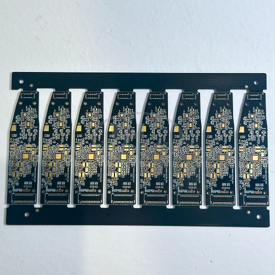
A process edge (also called a working edge, or tooling rail) is an auxiliary band reserved along the edge of a PCB, free of traces and components. It is not part of the circuit's electrical function — it is a process structure reserved specifically to support manufacturing, including panelization, transport, component placement, and testing.
2. Why Does a PCB Need a Process Edge?
There are two main reasons:
2.1 Panel connection needs
During volume production, PCBs are usually produced in panels (panelization). When spacing exists between individual boards, the process edge is what connects multiple small boards into one complete panel for downstream production. This improves efficiency and reduces cost.
2.2 Clamping needs during component placement
Equipment such as pick-and-place machines, wave soldering, and AOI (Automated Optical Inspection) must clamp the edge of the PCB to position and transport it during operation. The process edge provides a reliable clamping area for this equipment and is the foundation of a stable placement process.
3. How Does the Process Edge Work During Placement?
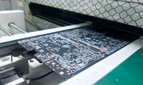
Take a pick-and-place machine as an example: when a PCB is transferred to the machine, the conveyor rail's clamp first grips the board edge to hold the PCB in place. The guide rail clamp holds roughly 3mm of the board edge, ensuring overall placement quality and stability.
Two key clearance recommendations:
- Avoiding collisions:To prevent components near the board edge from colliding with the machine's rail clamp, and to prevent collisions with other equipment during transport after placement, it is recommended that the distance between edge components and the rail clamp be kept at >2mm.
- Overall design recommendation:The distance between placed components and the PCB edge should be kept at ≥5mm.
If the distance between the PCB edge and components is <5mm, a process edge is recommended, with a recommended process edge width of ≥5mm.
4. Why Is the Process Edge Placed on the Long Side?
Throughout the transport process, boards are transported "vertically" (edge-leading) on the guide rails to ensure more stable handling through the equipment; feeding boards vertically also makes component placement more stable. Therefore, it is recommended to set the long side of the PCB as the process edge, aligning with the equipment's transport direction to keep the entire production line running smoothly.
5. Process Edge Design Recommendations at a Glance
| Design Item | Recommendation |
|---|---|
| Component-to-edge clearance | ≥5mm |
| Component-to-clamp clearance | >2mm |
| When a process edge is needed | Component-to-edge clearance <5mm |
| Recommended process edge width | ≥5mm |
| Process edge location | Long side of the PCB |
Though small, the process edge is a key part of ensuring smooth volume production and improving placement yield. Properly reserving a process edge at the design stage effectively avoids issues such as clamping collisions and unstable positioning, helping your products move smoothly from prototype to volume production.
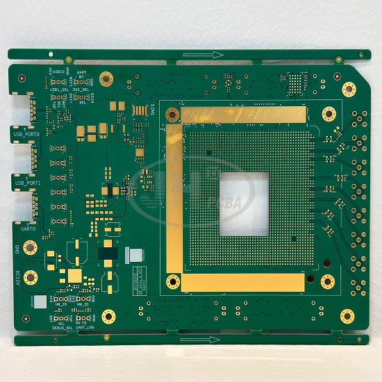
If you have any questions about PCB panelization and process edge design, feel free to contact us at [https://www.szjhpcba.com/](https://www.szjhpcba.com/). We will provide professional panelization and process edge solutions tailored to your board structure — visit [https://www.szjhpcba.com/pcba.html](https://www.szjhpcba.com/pcba.html) for more details.