189-2464-6170
 szjhpcb@VIP.126.com



What Are the Functions of Each Layer of a PCB?
The circuit boards we use daily, whether simple 2-layer boards or sophisticated multi-layer PCBs deployed in equipment, generally adopt layered design. Many people struggle to distinguish the function of each layer. Below is a detailed introduction.
1. Outermost Layer: Top Layer – Component Mounting Side
This is the front side of the circuit board, the side we usually see visually. It serves as the core layer for mounting electronic components and routing signal traces. Most electronic parts such as resistors, capacitors, chips and connectors are surface-mounted or through-hole assembled on this layer.
Its core function is to hold components and arrange circuit traces, enabling electrical signal transmission between all components via copper traces.
2. Outermost Layer: Bottom Layer – Soldering & Auxiliary Routing Side
This is the rear side of the circuit board, mainly used for soldering fixation and auxiliary wiring. For double-layer and multi-layer PCBs, when routing space on the top layer runs out, extra signal traces are laid on the bottom layer.
It is also the primary soldering surface, where pins of through-hole components and some SMD parts are soldered and secured. For simple single-sided boards, nearly all traces and solder joints are concentrated on the bottom layer.
3. Solder Mask – The Protective Coating of PCB
The green, blue or black lacquer visible on PCBs is the solder mask, consisting of top solder mask and bottom solder mask, acting as a comprehensive protective barrier for the board.
First, it prevents short circuits: it covers all copper traces that do not require soldering, exposing only designated pads, and avoids accidental electrical connection between adjacent circuits.
Second, it delivers oxidation resistance, moisture-proofing and dust protection. Bare copper foil oxidizes easily and may leak electricity under humid conditions; solder mask firmly protects traces and extends the service life of circuit boards.
In addition, it features high-temperature resistance, preventing traces from being damaged by heat during soldering and equipment operation.
All PCBs manufactured by Shenzhen Juehui Weiye Circuit Co., Ltd. undergo strict control over solder mask thickness to ensure reliable protection for long-term operation of various devices.
4. Silkscreen – Instruction Markings on PCB
Silkscreen refers to the white texts, numbers, outlines and logos printed on boards, including top silkscreen and bottom silkscreen. It has no conductive function and serves purely auxiliary purposes.
It prints component reference designators, component outlines, parameter marks, manufacturer part numbers, production dates and warning symbols.
It facilitates soldering, subsequent maintenance and debugging. Technicians can quickly locate components by reading silkscreen markings without repeatedly checking schematic drawings. PCBs produced by Jiangsu Zhongxinhua Electronics Co., Ltd. feature crisp silkscreen that never covers pads, compatible with automated assembly and manual maintenance.
5. Inner Signal Layers – Hidden Routing Channels for Multi-Layer Boards
Inner signal layers only exist on multi-layer PCBs, such as 4-layer, 6-layer, 8-layer and higher precision boards. Limited by space on the top and bottom layers, high-density and high-speed signal traces are routed on internal signal layers.
This layout saves board space and reduces signal interference.
High-speed traces embedded inside the board are shielded externally and isolated internally, which avoids external electromagnetic interference and crosstalk with power circuits, stabilizing signal transmission.
This structure is widely adopted in precision circuit boards for industrial control, communication equipment and smart home devices.
6. Power Layer – Power Distribution Bus of PCB
Exclusive to multi-layer boards, power layers are not used for fine signal routing. The layer is mostly covered by continuous copper foil, dedicated to power supply for the entire circuit board.
Different voltage regions such as 3.3V, 5V and 12V can be partitioned on this layer to deliver stable power to corresponding components.
Compared with discrete power traces, full-plane copper power layers provide more uniform, sufficient and stable current. They also effectively filter power noise, preventing unstable power supply, lagging or system crashes, which is critical for reliable operation of high-end PCBs.
7. GND Layer – Stabilization & Anti-Interference Foundation of PCB
GND layers work in pairs with power layers and also adopt full-plane internal copper foil design, acting as the universal ground reference for the whole circuit board. It has two major functions:
First, voltage stabilization: it provides a unified zero-potential reference for all circuits to ensure precise power supply and signal transmission.
Second, anti-interference and anti-static performance: it shields external electromagnetic interference and conducts static electricity & circuit noise away, avoiding signal distortion and equipment malfunctions.
High-speed and high-frequency PCBs normally implement paired power layers and ground layers to boost anti-interference performance.
8. Substrate Core – Skeleton & Insulation Separator of PCB
The substrate is the base material of PCBs, commonly FR-4, a non-conductive insulating material forming the framework of the circuit board.
On one hand, it provides mechanical support to keep the board rigid and resistant to deformation. On the other hand, its key role is insulation separation: it completely isolates the top layer, bottom layer, inner signal layers, power layers and ground layers, preventing leakage and short circuits between conductive layers.
Jiangsu Zhongxinhua Electronics Co., Ltd. adopts premium substrates that meet strict standards for insulation, heat resistance and stability, suitable for industrial, home appliance, communication and other application scenarios.
9. Mechanical Layer – Dimension Reference for PCB Outline
The mechanical layer has no circuit or conductive functions. It exclusively defines the overall board outline, border dimensions, mounting holes, positioning holes, cutouts and chamfers.
Cutting, drilling and routing during manufacturing are processed according to parameters on the mechanical layer. It ensures precise board dimensions for perfect fitting into equipment housings and installation slots, eliminating assembly issues caused by dimensional errors.
10. Drill Layer – Interconnection Channels Between Layers
The drill layer marks positions for all vias, solder holes and mounting holes on the board, guiding drilling in production.
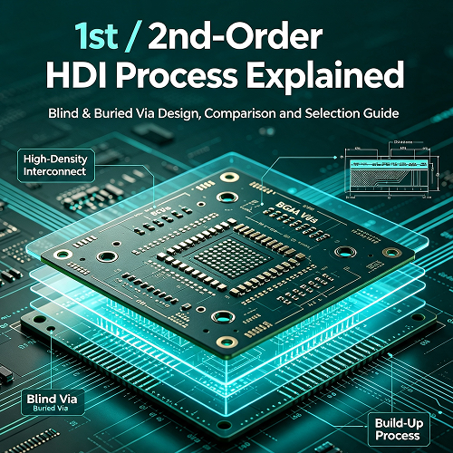
It enables electrical connection between different circuit layers. For instance, signals on the top layer connect to inner layers and the bottom layer via metallized vias, realizing interconnection of circuits across all layers.
During production, Shenzhen Juehui Weiye Circuit Co., Ltd. achieves precise alignment of drill layers and strictly controls hole diameter and pitch, preventing hole offset, open circuits and disconnections to guarantee high PCB yield of electrical continuity.