189-2464-6170
 szjhpcb@VIP.126.com



One-Stop Guide to PCBA Value-Added Services: Conformal Coating, Laser Marking, Firmware Programming & Testing/Burn-in
SMT placement and soldering is only the "first half" of a PCBA delivery. Before a product can go outdoors, into vehicles, or onto a medical production line, it must pass the gates of traceability, moisture protection, weather resistance, and functional verification. Built on small-to-medium-batch PCBA SMT customization, Juehui Weiye Circuits SMT provides a full range of post-assembly value-added services — conformal coating, board cleaning, laser marking, firmware programming, inspection & burn-in, BGA ball placement & rework, professional packaging, and depaneling & shipping — all through a single window, freely configurable on demand.
Juehui Weiye Circuits focuses on high-reliability sectors including medical electronics, automotive electronics, 5G communications, defense communications, and AI high-speed servers. We support 4–26 layer any-layer HDI, high multi-layer boards, rigid-flex boards, high-frequency boards, and high-speed boards, and professionally undertake special-process PCB prototyping and small-to-medium-batch manufacturing, including back-drilling, impedance control, hybrid material lamination, resin plugging, copper paste plugging, selective heavy hard gold, gold plating, 0.2 mm ultra-thin boards, heavy copper, and embedded capacitors/resistors. With 5 Yamaha high-speed SMT lines and advanced SPI, 3D solder paste inspection, inline AOI, and X-ray inspection equipment, we deliver highly reliable single- and double-sided SMT assembly for a wide range of PCBs, stably supporting high-precision miniature component placement down to 01005, 0201, BGA, and QFN. On top of full MES-based manufacturing traceability, we offer a complete suite of post-assembly value-added services — conformal coating, board cleaning, laser marking, firmware programming, inspection & burn-in, BGA ball placement & rework, professional packaging, and depaneling & shipping.
1. Conformal Coating: A "Protective Suit" for Your PCBA
What is conformal coating?
Conformal coating is a protective layer applied to the circuit board surface, delivering three key protections — moisture resistance, salt-spray resistance, and fungus resistance. It is a standard process for high-reliability products such as outdoor equipment, automotive electronics, and medical instruments.
- Material systems: Primarily high-performance UV-curable conformal coating; polyurethane, acrylic, and silicone systems are available per the product's operating environment;
- Coating thickness: Typically 50–200 μm, adjustable to the required reliability class;
- Application method: Front-side full-board spray by default; selective coating supported to precisely mask connectors, gold fingers, heat-dissipation areas, and other no-coat zones;
- Applicable scenarios: Outdoor equipment, energy storage and automotive electronics, medical devices, aerospace, 5G base stations, and other harsh or high-humidity environments.
2. Board Cleaning: The "Final Wipe" of a No-Clean Process
Most SMT plants run no-clean processes, where post-soldering residues are barely visible. After wave soldering of through-hole components, however, a transparent, slightly tacky flux residue can remain on the board. It does not affect electrical performance, but it can affect visual inspection and downstream processing.
We offer two professional cleaning options:
- Dry-ice cleaning: Physically strips residue with no water and no chemical residue — ideal for precision components and sensitive board surfaces; removes slightly tacky flux residue locally;
- Board-washing solvent cleaning: Thoroughly removes solder balls, fingerprints, dust, and other contaminants to meet visual inspection and higher cleanliness requirements.

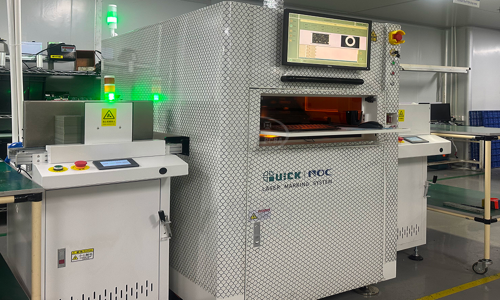
3. Laser Marking: One Board, One Code, Fully Traceable
To support product traceability and quality management, we provide PCB/PCBA laser marking services:
- Marking content: QR codes, 1D barcodes, serial numbers, batch numbers, logos, UDI codes, etc.;
- Process capability: CCD vision-aligned automatic marking — clear, wear-resistant, and durable, with minimum characters down to sub-millimeter level;
- System integration: Marking data can be uploaded to the MES manufacturing execution system for one-board-one-code full-lifecycle traceability — forward tracing to batch materials, reverse tracing to pinpoint failure points.
4. Firmware Programming: Firmware Written Before Boards Leave the Line
- Supported devices: MCU, Flash, memory ICs, and common programmable logic devices;
- Programming methods: In-circuit and off-line programming; encrypted programming and programming verification supported;
- Key advantages: Programming completed inside the SMT line reduces pin damage from secondary handling of ICs, prevents firmware/hardware version mismatches, and shortens the delivery chain.
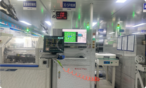
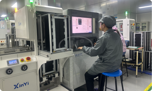
5. Inspection & Testing: Blocking Defects Before They Ship
| Process inspection | SPI solder paste inspection, AOI optical inspection, X-ray solder joint inspection | Solder paste printing quality; component placement and soldering defects; BGA/QFN bottom solder joints and void-rate inspection |
| Electrical testing | Flying probe test, ICT in-circuit test, FCT functional test | Open/short circuits, component parameters, full-board function and firmware-linked verification |
| Reliability testing | High-temperature burn-in, temperature cycling, MTBF aging screening; optional Hi-Pot insulation withstand test | Expose early-life failures in advance; suited to stringent industries such as automotive electronics and energy storage |
| Failure analysis | Cross-sectioning, dye & pry, thermal imaging (third-party laboratory support available) | Identify root causes of solder joint and device failures; feed improvements back into design |
6. BGA Ball Placement & Rework: High-Reliability Repair for Bottom-Pad Devices
- BGA ball placement, de-soldering & rework, IC lead cleaning & pin straightening, and tape & reel services;
- Post-rework X-ray re-inspection of ball coplanarity and solder joint quality ensures repair reliability;
- Suited to batch ball placement and single-unit rework of bottom-pad packages including BGA and QFN.

7. Packaging Services: Customized by Product Risk Level
- Standard packaging: Anti-static (ESD) bag plus red bubble wrap to protect against in-transit vibration;
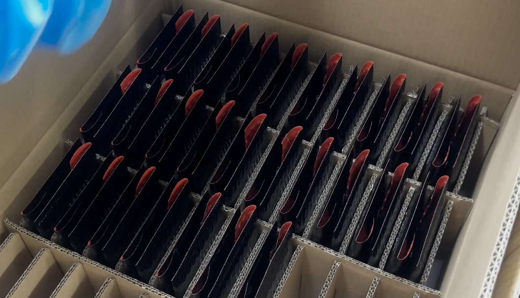
- Batch partition packaging: Boards separated by cardboard dividers and stood upright — pressure-resistant and minimizing compression between finished boards; ideal for taller or delicate components;
- Multi-layer protection: ESD bag + dividers + bubble wrap combination for extra assurance in courier shipping;
- Moisture-barrier packaging (optional): Vacuum moisture-barrier packaging with desiccant and humidity indicator cards, suited to moisture-sensitive devices (MSL-controlled).
8. Depaneling & Shipping: Panelized or Pre-Separated, Your Call
PCBA boards are often manufactured with process rails or in multi-up panels, and must be separated into individual units before final assembly. Using fixtures with dedicated depaneling machines, we support the following separation methods:
1. V-CUT scoring: A circular blade rolls and breaks along the V-groove — fast (100–200 mm/s) and low cost; however, limited to straight V-grooves, with some bending stress and burrs; suited to straight-line panels and high volume.
2. Guillotine depaneling: A blade presses straight down to cut — simple structure and fast; however, straight edges only and higher stress; suited to straight-edge panels.
3. Routing: A high-speed spindle router follows a programmed path — high precision, controllable stress, and capable of irregular contours; however, tooling wears and requires periodic replacement; suited to thick boards (>1.6 mm), automotive electronics, medical devices, and irregular panels.
4. Punch depaneling: Custom die stamps boards apart — extremely fast with clean edges; however, die cost is high and the cut path is fixed; suited to a single board type in very high volume.
5. Laser depaneling: UV/green laser non-contact ablation cutting — zero mechanical stress, kerf < 0.1 mm, no burrs, and any contour possible; suited to FPC flex boards, rigid-flex boards, ultra-thin boards (<0.4 mm), high-frequency/ceramic substrates, and BGA/MLCC stress-sensitive areas.
Selection guidance:
- Thick boards and automotive/medical applications with high reliability requirements: **routing** preferred — controllable stress, supports irregular contours;
- FPC flex, rigid-flex, ultra-thin boards, and dense BGA/MLCC areas: **laser depaneling** first choice — zero stress, no burrs, no secondary trimming;
- Regular straight-line panels, high volume, cost-sensitive: **V-CUT scoring** offers the highest efficiency;
- Single board type in very high volume: **punch depaneling** can be evaluated for the lowest per-unit cost.
Boards may be delivered panelized for self-depaneling by the customer, or we can separate and pack them as individual units before shipping.
Other Optional Services
Custom fabrication per drawing | Turnkey PCBA (materials + assembly) | Customer-supplied materials | DFM manufacturability analysis | First Article Inspection (FAI) | Box build (enclosures / cables / final packaging)
Pricing
Value-added services are quoted comprehensively based on process complexity, board area, and order quantity. Contact your dedicated Juehui Weye service specialist for direct coordination; volume orders enjoy preferential pricing.
Why Choose Shenzhen Juehui Weiye Circuit Co., Ltd.
- Small-to-medium-batch friendly: Seamless switching between prototyping, small-batch, and volume production, with dedicated one-on-one project support;
- Proven high-reliability process capability: 4–26 layer any-layer HDI, high multi-layer boards, rigid-flex boards, high-frequency boards, high-speed boards; professional capability in back-drilling, impedance control, hybrid material lamination, resin plugging, copper paste plugging, selective heavy hard gold, gold plating, 0.2 mm ultra-thin boards, heavy copper, and embedded capacitors/resistors;
- High-end industry track record: Serving customers in medical, defense communications, 5G communications, AI servers, automotive TBOX/eCall, and aviation navigation;
- One-stop single window: PCB fabrication + SMT assembly + value-added services + components — reducing multi-supplier coordination costs.
FAQ: Common Questions About PCBA Value-Added Services
Q1: What services are included in PCBA value-added services?
A: Conformal coating, board cleaning, laser marking, firmware programming, inspection & burn-in, BGA ball placement & rework, packaging, and depaneling & shipping — freely combinable on demand.
Q2: What is the typical conformal coating thickness?
A: Typically 50–200 μm, front-side spray by default. Selective coating is available when connectors, gold fingers, and other areas need to be masked.
Q3: Can laser-marked QR codes be used for product traceability?
A: Yes. QR codes, 1D barcodes, serial numbers, and UDI codes can all be laser-marked, and the marking data can be linked to the MES traceability system.
Q4: Do you support firmware programming? What do we need to provide?
A: Yes, we program MCU, Flash, and other ICs. You need to provide the firmware file and programming requirements (encryption, program address, and verification method).
Q5: How are value-added services priced?
A: Quoted on a per-project basis, with itemized quotes available. Services already live on our system can be configured online, and volume orders enjoy preferential pricing.
Q6: Can you source components, or use customer-supplied materials?
A: Yes. We support both component procurement and customer-supplied materials, with material status traceable throughout.
---
Need PCBA value-added services? Talk to Juehui Weiye Circuits today.
Tel: 【189-2464-6170】 Email: 【szjhpcb@vip.126.com】
Submit your BOM/Gerber for a free process evaluation and quotation.
This page is compiled by Juehui Weiye Circuits SMT based on its own service capabilities. Process parameters shown are typical ranges; final specifications are subject to technical confirmation of the order.