189-2464-6170
 szjhpcb@VIP.126.com



Research on Differential Signal Integrity Under Mesh Copper Misalignment|PCB Manufacturing Tolerance & SMT Mass Production Design Guidelines
Meshed reference planes are widely used to optimize differential insertion loss in high-speed PCB and FPC designs. However, mesh copper misalignment introduced during PCB exposure and lamination causes impedance imbalance within differential pairs and deteriorates signal integrity. Based on full-wave simulation, Juehui PCB / Juehui PCBA compares the insertion loss performance of differential structures with different trace widths and spacings under mesh shift. Combined with PCB manufacturing tolerance and SMT test requirements, we provide PCB prototyping, high-precision SMT assembly and mass PCBA production services for automotive, computing and industrial high-speed differential links.
Applicable scenarios: High-speed PCB, FPC flexible circuits, automotive, computing, industrial high-frequency differential link design. Target readers: Hardware engineers and SI (Signal Integrity) engineers. This guideline balances PCB fabrication and SMT assembly process implementation.
In high-speed circuit and FPC flexible circuit design, the meshed reference layer (meshed copper ground) is a widely adopted engineering solution. It balances power integrity, thermal dissipation and differential insertion loss, and is extensively applied in high-frequency communication, AI computing boards, automotive domain controllers and industrial control products.
Nevertheless, inherent process deviations exist during PCB/FPC manufacturing. Mesh copper etching, alignment exposure and lamination will lead to mesh copper misalignment, meaning the relative position between the meshed reference plane and differential traces shifts. This misalignment directly creates inconsistent impedance between the two traces in a differential pair, breaks differential coupling balance, introduces mode conversion and degrades differential insertion loss. In severe cases, it triggers bit errors and instability of high-speed links.
Juehui Weiye Circuit provides one-stop PCBA services including high-speed PCB & FPC fabrication and SMT assembly. To address this common industry pain point, we carry out special research on the impact of mesh copper misalignment on differential signal integrity using 3D full-wave simulation and real production process boundaries. We deliver practical design rules for customers’ high-speed differential routing, fully compatible with PCB manufacturing and SMT process control requirements.
1. Background & Principle
Differential signals are transmitted via coupled trace pairs. Compared with single-ended signals, they feature strong noise immunity, crosstalk suppression and good tolerance to discontinuities, making them the mainstream solution for high-speed SerDes, DDR and high-speed interfaces.
Most existing studies on meshed copper reference planes focus on static impedance calculation, ignoring differential coupling imbalance induced by manufacturing misalignment. After mesh copper shifts, the reference ground environment for the two traces inside a differential pair becomes asymmetric. It alters single-ended impedance and changes differential coupling strength at the same time. The combined effect worsens insertion loss, a frequently overlooked risk in high-frequency SI design.
The substrate stack-up adopted in this simulation consists of double-sided FCCL (FPC) + adhesive + single-sided FCCL. Stack parameters strictly follow FPC mass production specifications:
- Copper of double-sided FCCL: 12 μm, modified polyimide (MPI)
- Substrate of double-sided FCCL: 25 μm, MPI
- Adhesive: 20 μm, low-loss pure adhesive
- Copper of single-sided FCCL: 12 μm, MPI
Target differential impedance of the simulated differential traces: 85 Ω; trace length: 100 mm. Fixed geometric parameters of mesh copper: mesh line width \(L_W\)=125 μm, mesh pitch \(S_P\)=175 μm.
Three typical differential routing cases covering common trace width & spacing combinations in engineering are set up for comparison:
- Case1: Trace width 54 μm, trace spacing 77 μm (spacing > width, <2×width)
- Case2: Trace width 54 μm, trace spacing 45 μm (spacing < width, tighter coupling)
- Case3: Trace width 58 μm, trace spacing 154 μm (width + spacing ≈ mesh diagonal distance, special aligned layout)
Unified misalignment setup: The mesh copper shifts leftward by 20/40/60/80/100 μm relative to the centered differential pair, simulating process offset from PCB/FPC exposure alignment and lamination. This offset range represents typical manufacturing deviation for FPC and thin-core PCB mass production.
>
> Process Note: Mesh misalignment mainly originates from PCB/FPC exposure deviation, lamination slippage and dry film alignment error. SMT assembly will not directly change the relative position of mesh copper. However, if no misalignment margin is reserved in early SI design, high-speed signal failures will be found in functional tests after SMT, resulting in extra rework and board replacement costs.
2. Simulation Results & Rule Interpretation
2.1 Case1 (Trace width 54 μm, spacing 77 μm)
As mesh copper offset increases, differential insertion loss **drops first then rises**, while differential impedance keeps increasing.
Root cause: At the initial stage of offset, coupling variation brings loss improvement. As the offset continues to grow, the single-ended impedance difference between the two traces in the differential pair keeps expanding. Impedance imbalance becomes the dominant factor and insertion loss deteriorates rapidly.
Single-ended simulation data shows that larger offset leads to greater impedance difference between the two traces, which aggravates loss degradation under differential mode.
2.2 Case2 (Trace width 54 μm, spacing 45 μm, tightly coupled differential)
Tightly coupled differential pairs have stronger coupling between traces.
Under the same mesh offset conditions, insertion loss follows the same trend as Case1 (decrease first then increase), but with **smaller fluctuation range** and better resistance to mesh misalignment.
Mechanism: The coupling between differential traces dominates, weakening the asymmetric effect introduced by meshed reference layer shift. It offers better tolerance and suits high-speed links requiring stable loss performance.
2.3 Case3 (Trace width 58 μm, spacing 154 μm, special aligned layout)
This layout has weaker coupling strength than Case1 and Case2, yet the traces are specially aligned with the mesh copper, which effectively suppresses impedance imbalance caused by mesh shift.
When mesh copper is offset, the impedance of the two traces in the differential pair remains nearly identical and the impedance difference is close to zero. Insertion loss no longer follows the “drop-first-then-rise” trend. Instead, loss rises slightly after offset, while impedance consistency remains excellent and signal integrity stays stable.
>
> Engineering Value: This routing scheme is the preferred option for differential design with meshed reference planes. It provides extremely high tolerance against PCB alignment offset and is suitable for mass projects with strict consistency requirements.
2.4 Summary Comparison (Differential Insertion Loss @15 GHz)
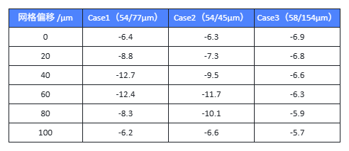
It can be clearly observed that:
1. Case1 and Case2 suffer severe loss degradation under medium offset, carrying high mass-production fluctuation risks;
2. Case3 shows gentle loss variation with rising offset and delivers optimal process robustness.
3. Engineering Design Recommendations Combined with PCB Fabrication & SMT Assembly
Combining simulation results and in-house process capability, Juehui Weiye Circuit releases mass-production-oriented design specifications balancing SI performance, PCB yield and SMT first-pass test rate:
1. Prioritize the Case3 layout strategy: Match the sum of differential trace width and spacing to the mesh diagonal distance, placing differential traces at special symmetric positions of the mesh copper. This eliminates impedance imbalance induced by mesh alignment offset from the design stage and reduces SI risks from exposure and lamination deviation. Ideal for high-reliability products such as automotive and computing hardware.
2. Tightly coupled differential (Case2) for high stability requirements: If layout space is limited, tight coupling improves anti-offset capability. Meanwhile, PCB etching tolerance must be controlled to guarantee consistent width of the two traces. Superposition of etching deviation and mesh offset will further amplify impedance unbalance.
3. Define process boundaries in advance: Specify mesh copper alignment tolerance in PCB fabrication specifications, confirm the maximum exposure and lamination offset with the manufacturer in advance. Run margin simulation based on the factory’s actual maximum offset instead of only simulating the ideal centered mesh.
4. Coordinated SMT test control: High-speed boards are recommended to add high-speed eye diagram and insertion loss sampling tests after SMT. Conventional loosely coupled differential design (Case1) has a narrow process window. SI verification on small-batch prototypes is suggested before mass assembly to avoid batch failures.
5. Supplementary rules for mesh copper design: Mesh opening size, copper thickness and etching compensation shall be included in SI simulation. Avoid arbitrary local modification of mesh copper. Partial mesh gaps will alter the reference plane and amplify differential imbalance together with offset effects.
4. Conclusion
Misalignment of meshed reference planes is a non-negligible process-induced effect in high-speed PCB/FPC design. It breaks the impedance balance of differential pairs, changes coupling status and ultimately affects insertion loss.
- Conventional loosely coupled differential: Sensitive to mesh offset, loss fluctuates greatly with offset;
- Tightly coupled differential: Gains better anti-offset capability relying on trace-to-trace coupling;
- Specially aligned differential layout (Case3): Significantly suppresses impedance mismatch caused by mesh shift, delivers the most stable signal integrity and the best mass-production tolerance.
Juehui Weiye Circuit delivers one-stop PCBA services including high-speed PCB and FPC manufacturing, SMT assembly. We customize differential routing and meshed reference plane solutions according to your product frequency, impedance target and process capability. We balance signal integrity and mass yield while retaining layout flexibility, providing reliable one-stop PCB & PCBA manufacturing solutions for automotive, AI computing, industrial control and high-frequency communication high-speed links.
About Juehui Weiye Circuit
Juehui Weiye Circuit specializes in R&D and manufacturing of high-layer high-end PCB, HDI and FPC flexible circuits, paired with SMT assembly and one-stop PCBA services. We focus on high-speed signal design, impedance control and high-frequency material processes. We provide preliminary SI simulation, stack-up evaluation and DFM review to help customers achieve first-pass success for high-speed hardware products.